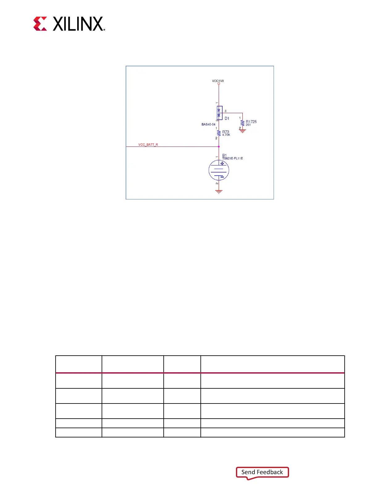
Figure 5: Encryption Key Backup Circuit
X23376-112420
The Seiko TS621E rechargeable 1.5V lithium buon-type baery B1 is soldered to the board
with the posive output connected to the XCVC1902 ACAP U1 VCC_BATT bank pin AG33. The
baery supply current IBATT specicaon is 150 nA maximum when board power is o. Baery
B1 is charged from the VCC1V8 1.8V rail through a 2 series diode with the rst forward drop to
yield between 0.24V to 0.46V over temperature per xed 5 mA load, R1725, and liming 1.56V
max at the ACAP pin, PSVBATT. The second diode and 4.7 kΩ current limit resistor allows the
baery to trickle charge and prevent baery B1 from back powering R1725.
I/O Voltage Rails
The XCVC1902 ACAP PL I/O bank voltages on the VCK190 board are listed in the following
table.
Note: The VCK190 board is shipped with VADJ_FMC set to 1.5V by the ZU4 system controller.
Table 6: I/O Voltage Rails
ACAP (U1)
Bank
Power Supply Rail
Net Name
Voltage Description
HDIO Bank 306 VCC1V8 1.8V GPIO: PB[0:1], DIP_SW[0:3], LED[0:3]; DC_PL_GPIO[0:3];
SYSCTLR_GPIO[0:5]; UART1_TXD/RXD
HDIO Bank 406 VCC3V3 3.3V HDMI status/ctrl(15)IF; HDIO_UART3_TX/RX;
HDIO_UART4_TX/RX
XPIO Bank 700 VCC1V2_DDR4 1.2V DDR4_DIMM1_DQ[32:63], CB[0:7], ADDR/CTRL;
DDR4_DIMM1_CLK; Si570 U2 200 MHz
XPIO Bank 701 VCC1V2_DDR4 1.2V DDR4_DIMM1_DQ[24:31], ADDR/CTRL
XPIO Bank 702 VCC1V2_DDR4 1.2V DDR4_DIMM1_DQ[0:23], CB[0:7]
Chapter 3: Board Component Descriptions
UG1366 (v1.0) January 7, 2021 www.xilinx.com
VCK190 Board User Guide 24

 Loading...


