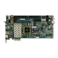
The VCK190 board has an I2C programmable SI570 low-jier 1.8V CMOS single-ended
oscillator (U32). The 33.333 MHz REF_CLK clock signals is connected to XCVC1902 ACAP U1
conguraon bank 503 pin AE32. At power-up, this clock defaults to an output frequency of
33.333 MHz. User applicaons or the System Controller can change the output frequency within
the range of 10 MHz to 945 MHz through the I2C bus interface. Power cycling the VCK190
board reverts this user clock to the default frequency of 33.333 MHz.
• Programmable oscillator: Silicon Labs SI570JAC000900DG (10 MHz-945 MHz range, 33.333
MHz default)
• I2C address 0x5D
• CMOS single-ended output, total stability: 61.5 ppm
Programmable SI5332 System Controller Clock
[Figure 3, callout 43]
The VCK190 board has an I2C programmable SI5332 low-jier 6-dierenal-output clock
generator (U142). Each output clock P/N pair has its own independent Vout pin. Two of the six
output clocks are used on the VCK190.
OUT0 is a single-ended 33.333 MHz 1.8V LVCMOS clock SYSCTLR_PS_REF_CLK connected to
the XCZU4EG System Controller (U125) conguraon bank 503 pin R16.
OUT1 is a dierenal 125.000 MHz 3.3V LVDS clock. The SYSCTLR_GTR_CLK0_SGMII_P and
SYSCTLR_GTR_CLK0_SGMII_N series capacitor coupled clock signals are connected to
XCZU4EG U125 GTR bank 505 MGTREFCLK0 pins F23 and F24, respecvely.
At power-up, OUT0 and OUT1 default the frequencies indicated above. User applicaons or the
System Controller can change the output frequency within the range of 0 MHz to 333.333 MHz
through the I2C bus interface. Power cycling the VCK190 board reverts the OUT0 and OUT1
frequencies to their defaults.
• Programmable clock generator: Silicon Labs Si5332FD10259-GM1 (0 MHz-333.333 MHz
range)
• Outputs
○ OUT0: 33.3333... MHz [33 + 1/3 MHz] LVCMOS Single (+) 1.8V 50Ω [100/3 MHz]
○ OUT1: 125 MHz LVDS slow 3.3V
○ OUT2: 26 MHz LVDS slow 3.3V
○ OUT3: Unused
○ OUT4: Unused
○ OUT5: Unused
Chapter 3: Board Component Descriptions
UG1366 (v1.0) January 7, 2021 www.xilinx.com
VCK190 Board User Guide 48
 Loading...
