GTY200: QSFP1
The GTY200 channels 0:3 are wired to QSFP1 J288.
The GTY200 REFCLK0 drives 8A34001_CLK1_IN, and REFCLK1 receives the
8A34001_Q1_OUT to and from the 8A34001 clock device U219.
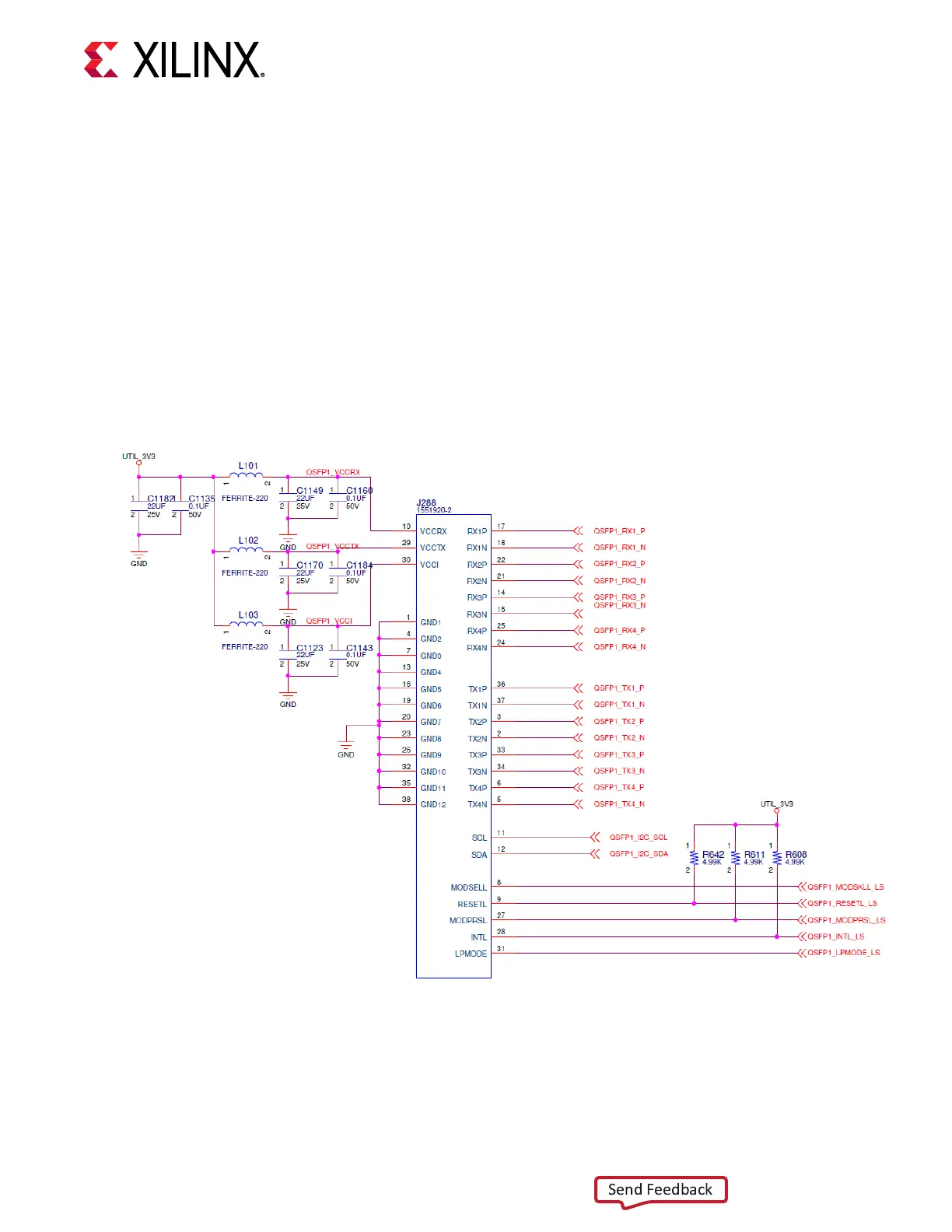
QSFP Module Connector
[Figure 3, callout 14]
The following gure shows the QSFP module connector circuitry implementaon.
Figure 21: QSFP Module Connector
X24954-121420
The QSFP connector 3.3V control nets are wired to ACAP U1 bank 406.
The QSFP connector I2C interface is connected to the I2C bus via the TCA9548 I2C mulplexer
U214 (see PMC MIO[44:45] I2C1 Bus for more details).
Chapter 3: Board Component Descriptions
UG1366 (v1.0) January 7, 2021 www.xilinx.com
VCK190 Board User Guide 55

 Loading...


