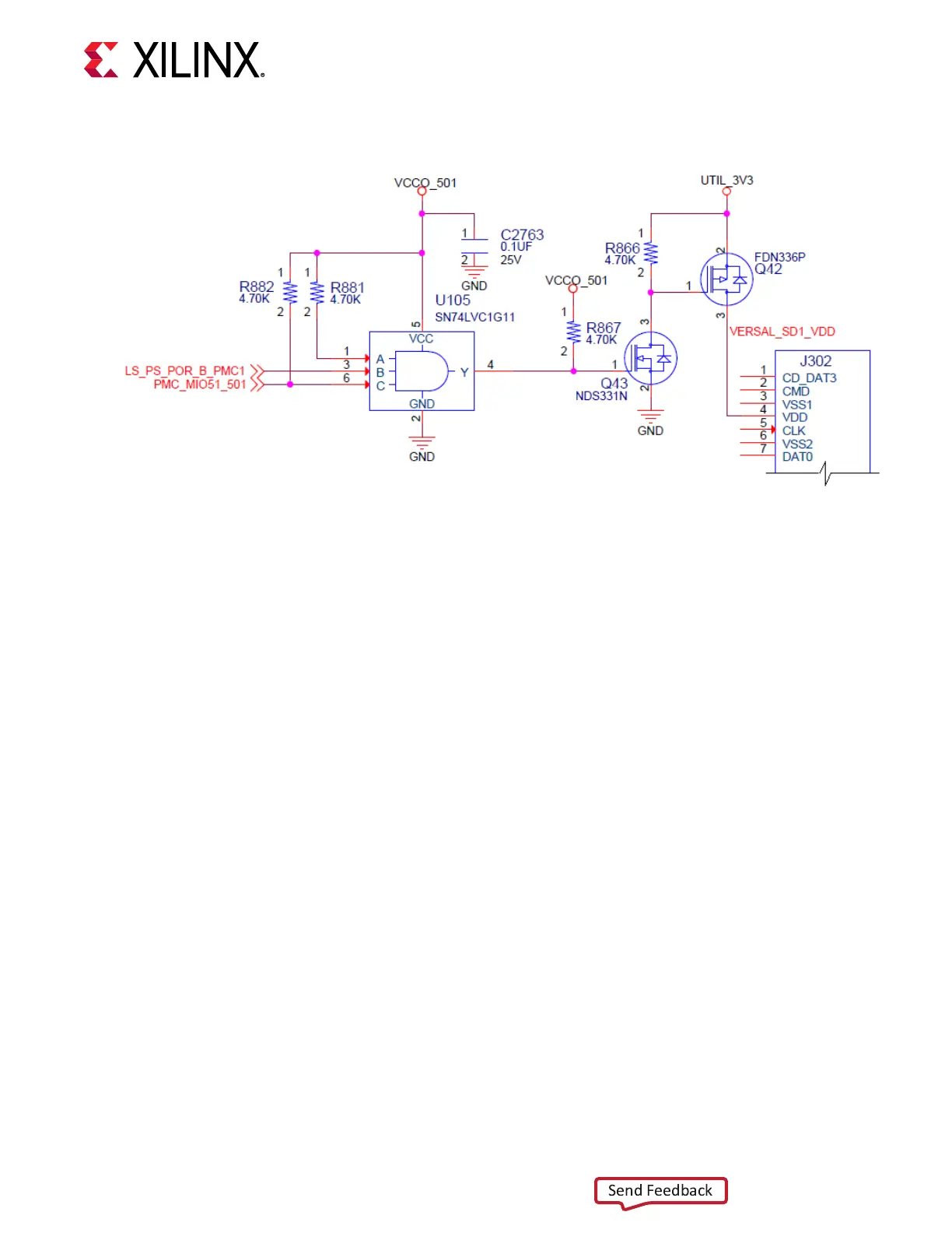
Figure 11: SD Socket J302 Power Control
X24951-121420
Informaon for the SD I/O card specicaon can be found at the SanDisk Corporaon or SD
Associaon websites. The VCK190 SD card interface supports the SD1 (2.0) and SD2 (3.0)
conguraon boot modes documented in the Versal ACAP Technical Reference Manual (AM011).
For Nexperia IP4856CX25 component details, see the IP4856CX25 data sheet at the Nexperia
website.
The detailed ACAP connecons for the feature described in this secon are documented in the
VCK190 board XDC le, referenced in Appendix B: Xilinx Design Constraints.
PS MIO[37] ZU4 System Controller GPIO
The ACAP PS bank 501 MIO37 is connected to the ZU4 system controller U125 bank 500
MIO11 pin AE17.
PMC MIO[38:39] PCIe Status
The ACAP PS bank 501 MIO38 (PCIE_PERST_B) and MIO50 (PCIE_WAKE_B) are connected to
the PCIe 8-lane edge connector P3 PERST# (pin A11) and WAKE# (pin B11), respecvely.
PMC MIO[40:41] CAN1
[Figure 3, callout 25]
Chapter 3: Board Component Descriptions
UG1366 (v1.0) January 7, 2021 www.xilinx.com
VCK190 Board User Guide 33

 Loading...


