The ACAP PS bank 501 MIO40 (TX OUT) and MIO41 (RX IN) support the PS-side CAN bus TX
and RX interface wired through the TI SN74AVC2T244 level-translators U107 and U109,
respecvely, to the NXP TJA1057GT/3J CAN-bus transceiver U110. This transceiver is
connected to the 2x4 0.1-inch pitch 8-pin male header J5.
See the NXP TJA1057GT/3J data sheet at the Nexperia website for CAN-bus transceiver details.
The detailed ACAP connecons for the feature described in this secon are documented in the
VCK190 board XDC le, referenced in Appendix B: Xilinx Design Constraints.
PMC MIO[42:43] UART0
[Figure 3, callout 8]
This is the primary Versal ACAP PS-side UART interface. The VCK190 USB Type-C connector
J207 only supports USB2.0.
MIO42 (RX_IN) and MIO43 (TX_OUT) are connected to FTDI FT4232HL U20 USB-to-Quad-
UART bridge port BD through TI SN74AVC4T245 level-shiers U18 and U21. The FT4232HL
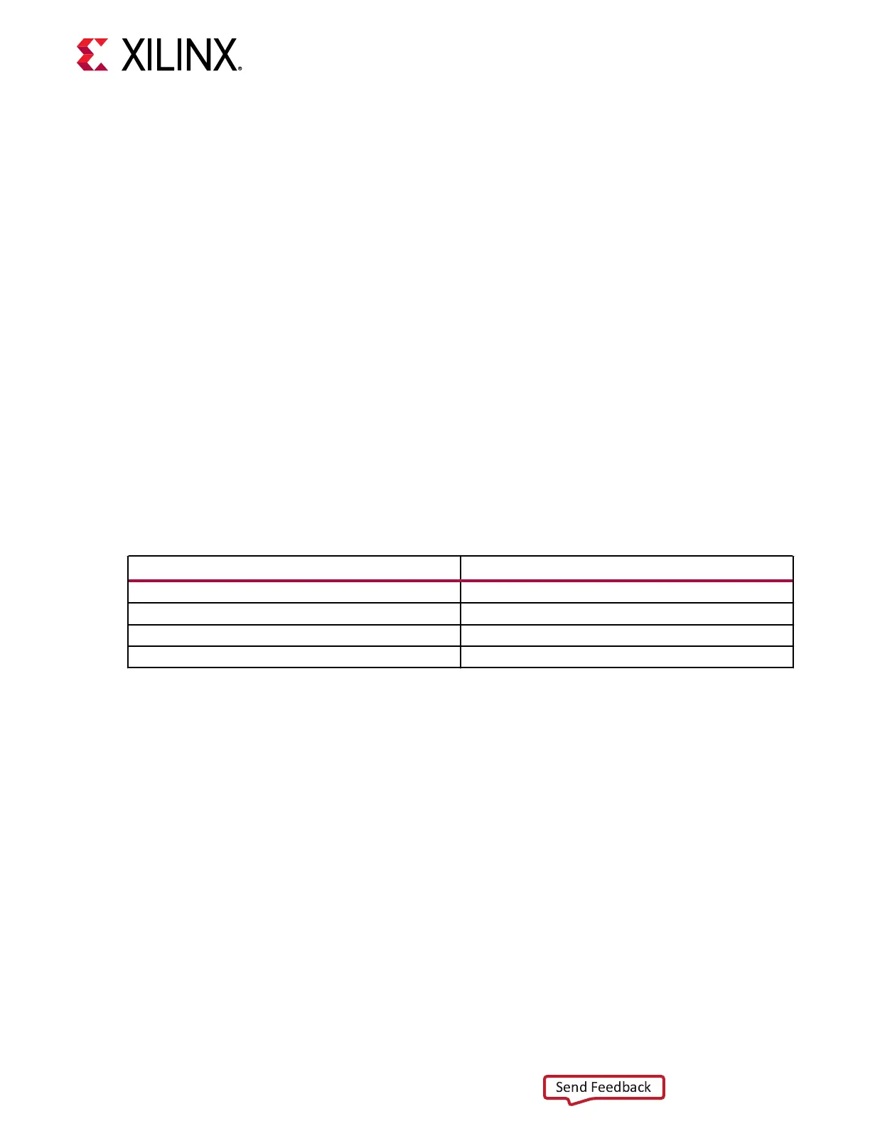
U20 port assignments are listed in the following table.
Table 9: FT4232HL Port Assignments
FT4232HL U34 Versal ACAP U1
Port AD JTAG VCK190 JTAG chain
Port BD UART0 PS_UART0 (MIO 18-19)
Port CD UART1 PL_UART1 bank 306
Port DD UART2 U20 system controller UART
The FT4232HL UART interface connecons are shown in the following gure.
Chapter 3: Board Component Descriptions
UG1366 (v1.0) January 7, 2021 www.xilinx.com
VCK190 Board User Guide 34

 Loading...


