The detailed ACAP connecons for the feature described in this secon are documented in the
VCK190 board XDC le, referenced in Appendix B: Xilinx Design Constraints.
GTY106: HDMI TX and RX
HDMI Video Output (TX)
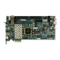
[Figure 3, callout 18 and 19]
The VCK190 board provides an HDMI™ video output using a TI SN65DP159RGZ HDMI remer
at U43. The HDMI output is provided on a TE Connecvity 1888811-1 right-angle dual-stacked
HDMI type A receptacle at P2 (upper port). The SN65DP159RGZ device is a dual mode
DisplayPort to transion-minimized dierenal signal (TMDS) remer supporng digital video
interface (DVI) 1.0 and HDMI 1.4b and 2.0 output signals. The SN65DP159RGZ device supports
the dual mode standard version 1.1 type 1 and type 2 through the DDC link or AUX channel. The
SN65DP159RGZ device supports data rates up to 6 Gb/s per data lane to support Ultra HD (4K
x 2K/60 Hz) 8-bits per color high-resoluon video and HDTV with 16-bit color depth at 1080p
(1920 x 1080/60 Hz). The SN65DP159RGZ device can automacally congure itself as a re-
driver at data rates <1 Gb/s, or as a remer at more than this data rate. This feature can be
turned o through I2C programming. The HDMI video transmit/receive block diagram is shown
in the following gure.
The ACAP U1 bank 406 user logic can implement a clock recovery circuit and output the series
resistor coupled HDMI_REC_CLK_OUT (pin L19) for jier aenuaon. The jier aenuated U62
Q2 HDMI_8T49N241_OUT_P/N series capacitor coupled output clock is connected to the
HDMI_TX/RX[0:3] interface GTY106 GTY_REFCLK1 pins E39 (P) and E40 (N).
Chapter 3: Board Component Descriptions
UG1366 (v1.0) January 7, 2021 www.xilinx.com
VCK190 Board User Guide 56
 Loading...
