EasyManua.ls Logo

Xilinx VCK190 Series User Manual

Xilinx VCK190 Series
79 pages
To Next Page IconTo Next Page
To Previous Page IconTo Previous Page
Page #42 background image
A PS Gigabit Ethernet MAC (GEM) implements a 10/100/1000 Mb/s Ethernet interface (see the
gure in PMC MIO[49] and LPD_MIO[12:25]: GEM1 Ethernet), which connects to TI
DP83867IRPAP U198 Ethernet RGMII PHY before being routed to a vercal dual-stacked RJ45
Ethernet connector J307 (upper receptacle). The RGMII Ethernet PHY is boot strapped to PHY
address (0x01) and Auto Negoaon is set to Enable.
PMC MIO[49] and LPD_MIO[12:25]: GEM1 Ethernet
[Figure 3, callout 17]
A PS Gigabit Ethernet MAC (GEM) implements a 10/100/1000 Mb/s Ethernet interface (see the
following gure), which connects to TI DP83867IRPAP U134 Ethernet RGMII PHY before being
routed to a vercal dual-stacked RJ45 Ethernet connector J307 (lower receptacle). The RGMII
Ethernet PHY is boot strapped to PHY address (0x02) and Auto Negoaon is set to Enable.
The following gure shows the dual Ethernet topology.
Figure 16: Dual RGMII Ethernet
XCVC1902
ACAP
RGMII
LPD MIO[0:11 24:25] LPD MIO[12:23 24:25]
GEM0 U198
DP83867IR
10/100/1000
PHY
MDIO
RGMII
GEM1 U134
DP83867IR
10/100/1000
PHY
MDIO
MII
J307
Upper
RJ45
J307
Lower
RJ45
25 MHz
Crystal
MII
25 MHz
Crystal
X23203-100119
Ethernet PHY (Three Resets)
[Figure 3, callout 35]
Each DP83867ISRGZ PHY (GEM0 U198, GEM1 U134) is reset by its GEMx_RESET_B generated
by dedicated pushbuon switches and PMC_MIO signals as shown in the following gure. The
POR_B signal generated by the TPS389001DSER U10 POR device (acvated by pushbuon
SW2) is wired in parallel to each Ethernet PHY reset circuit.
Chapter 3: Board Component Descriptions
UG1366 (v1.0) January 7, 2021 www.xilinx.com
VCK190 Board User Guide 42
Send Feedback

Table of Contents

Question and Answer IconNeed help?

Do you have a question about the Xilinx VCK190 Series and is the answer not in the manual?

Xilinx VCK190 Series Specifications

General IconGeneral
ManufacturerXilinx
SeriesVCK190
FPGA FamilyVersal
MemoryDDR4
PCIeGen4 x16
ChipsetVersal
StorageSATA
USB PortsUSB 3.0

Summary

Introduction to VCK190 Evaluation Board

VCK190 Overview

Introduces the VCK190 evaluation board and its capabilities.

Navigating Content by Design Process

Explains how the document is organized by design processes.

Additional Resources for VCK190

Lists external documents and resources for further information.

VCK190 Block Diagram

Provides a high-level visual representation of board components.

VCK190 Board Features

Details the key hardware features and capabilities of the VCK190 board.

VCK190 Board Specifications

Outlines the physical dimensions and environmental operating parameters.

Board Setup and Configuration

Standard ESD Measures

Provides essential precautions for handling electronic components safely.

Board Component Location

Identifies the physical locations of components on the VCK190 board.

Default Jumper and Switch Settings

Specifies the default configurations for jumpers and switches.

Versal ACAP Configuration

Details the boot modes and configuration options for the Versal ACAP.

Board Component Descriptions

Overview of Components

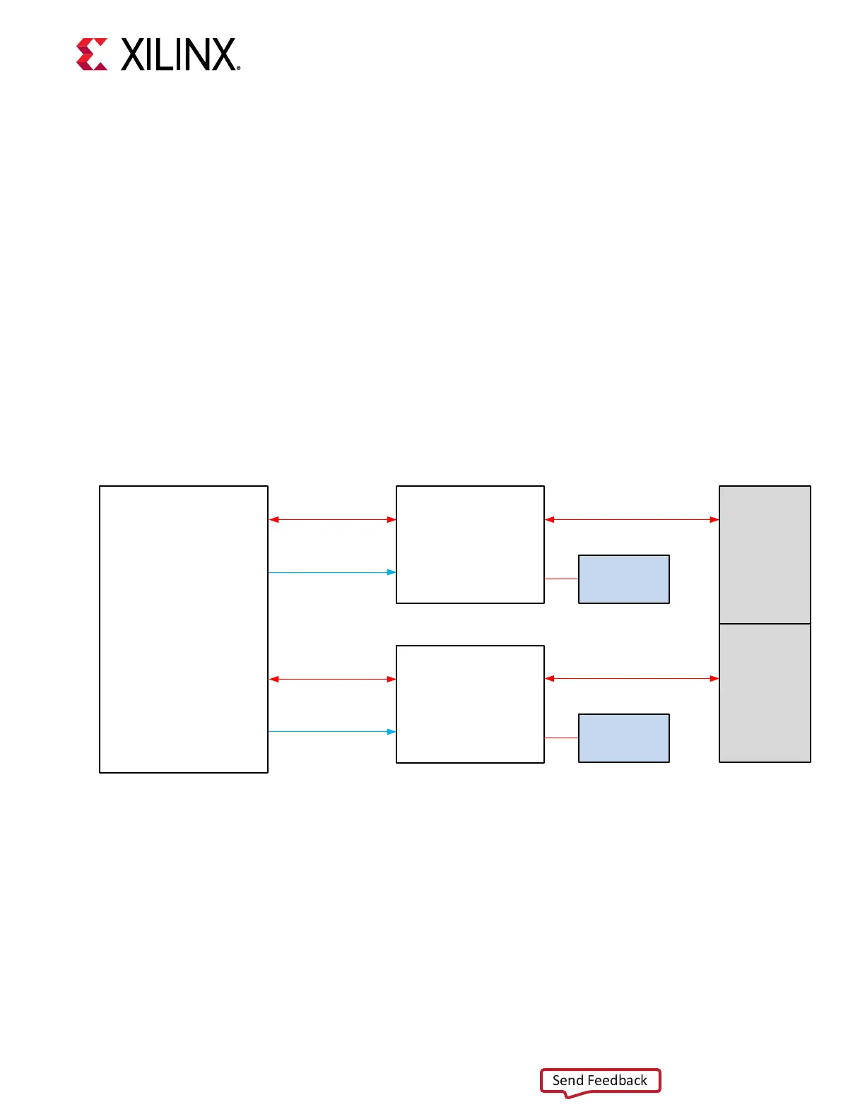
Provides a detailed functional description of board components and features.

Versal ACAP and Memory

Describes the Versal ACAP, DDR4 UDIMM, and LPDDR4 memory systems.

Interfaces and Connectivity

Details MIO, USB, SD, CAN, UART, I2C, and Ethernet interfaces.

Clocking and Transceivers

Covers clock sources, GTY transceivers, PCIe, FMC, SFP, QSFP, and HDMI.

Power Management and Control

Explains power rails, LEDs, fan control, system controller, and switches.

VITA 57.4 FMCP Connector Pinouts

Overview of FMCP Connectors

Introduces the FMC+ connector pinout defined by VITA 57.4.

FMCP HSPC Connector Pinout

Details the pinout of the FPGA Mezzanine Card (FMC) HSPC connector.

Xilinx Design Constraints

Overview of XDC Files

Explains the purpose and usage of XDC files for the VCK190 board.

XDC File Information

Provides guidance on using XDC files for VCK190 board designs.

Pmod FMC

Pmod FMC Overview

Introduces the Pmod FMC board for accessing Pmod devices.

Pin Mapping Pmod to FMC

Details the mapping between Pmod and FMC connector pins.

Regulatory and Compliance Information

CE Information

Lists relevant EU directives and standards for CE compliance.

Compliance Markings

Explains WEEE, RoHS, and CE compliance markings.

Additional Resources and Legal Notices

Xilinx Resources

Provides links to support resources like Answers, Docs, and Forums.

Documentation Navigator and Design Hubs

Explains how to access Xilinx documents and design resources.

References

Lists supplemental documents and external resources for the VCK190.

Important Legal Notices

Contains disclaimers, warranty information, and usage terms.

Related product manuals