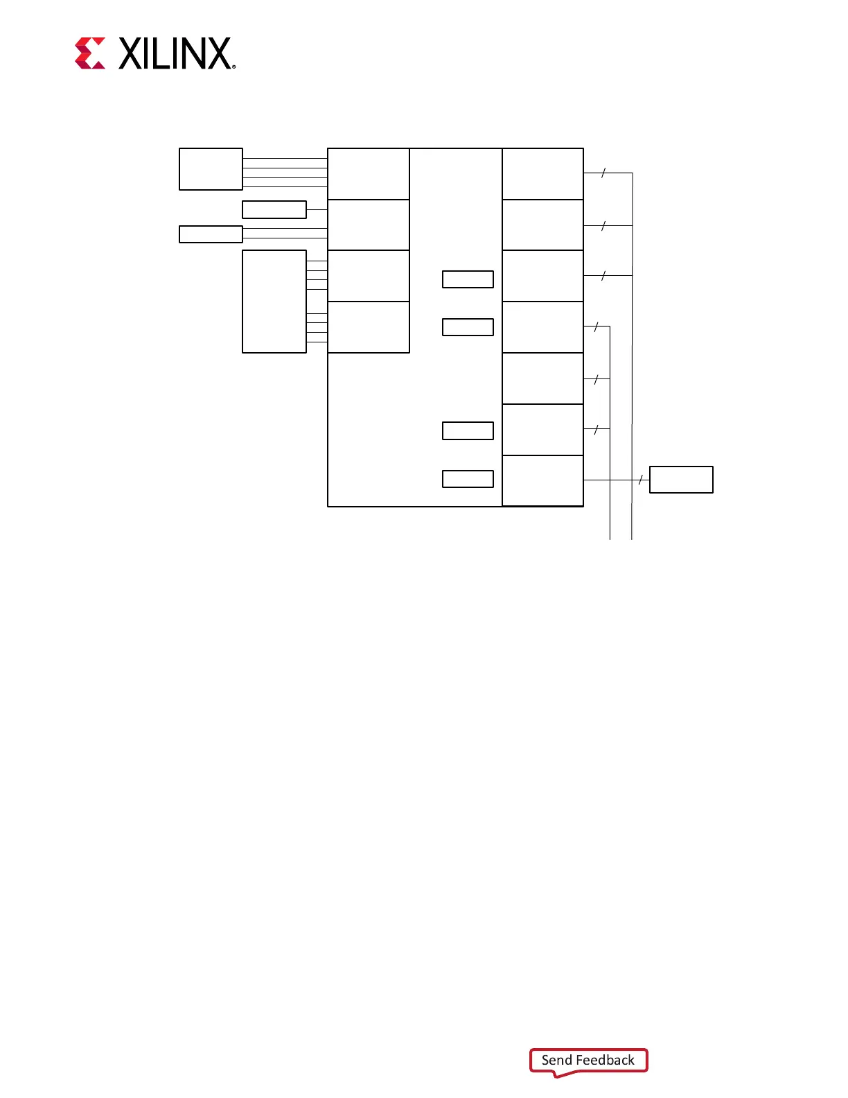
Figure 19: VCK190 GTY Connections
GTY0
GTY1
GTY2
GTY3
GTY
Bank 106
GTY0
GTY1
GTY2
GTY3
GTY
Bank 105
GTY0
GTY1
GTY2
GTY3
GTY
Bank 104
GTY0
GTY1
GTY2
GTY3
GTY
Bank 103
GTY0
GTY1
GTY2
GTY3
GTY
Bank 206
GTY0
GTY1
GTY2
GTY3
GTY
Bank 205
GTY0
GTY1
GTY2
GTY3
GTY
Bank 204
GTY0
GTY1
GTY2
GTY3
GTY
Bank 203
GTY0
GTY1
GTY2
GTY3
GTY
Bank 202
GTY0
GTY1
GTY2
GTY3
GTY
Bank 201
GTY0
GTY1
GTY2
GTY3
GTY
Bank 200
MRMAC
MRMAC
MRMAC
MRMAC
HDMI
HSDP
2x zSFP
Lane 4
Lane 5
Lane 6
Lane 7
PCIe
GEN4
x8
Lane 0
Lane 1
Lane 2
Lane 3
zQSFP
4
4
4
4
4
4
4
FMC+_01 FMC+_02
X23205-120120
GTY103/104: PCI Express Card Edge Connectivity
[Figure 3, callout 15]
The 8-lane PCI Express card edge connector P3 supports operaon up to Gen4 x8. P3 supports
data transfers at the rate of 2.5 GT/s for Gen1 applicaons, 5.0 GT/s for Gen2 applicaons, 8.0
GT/s for Gen3 applicaons, and 16.0 GT/s for Gen4 applicaons. The PCIe transmit and receive
signal data paths have a characterisc impedance of 85Ω ±10%. The PCIe_EP_REFCLK_P/N PCIe
reference clock (routed as a 100Ω dierenal pair) received from J18 is routed to IDT
85411AMLF U39 1:2 buer, which retransmits the clock as PCIe_CLK0 and PCIe_CLK1. U39
output Q0 PCIe_CLK0_P/N is routed to GTY103 (PCIe_EP_TX/RX[3:0]_P/N) and output Q1
PCIe_CLK1_P/N is routed to GTY104 (PCIe_TX/RX[7:4]_P/N).
For addional informaon about the Versal ACAP PCIe funconality, see the Versal ACAP
Integrated Block for PCI Express LogiCORE IP Product Guide (PG343). Addional informaon about
the PCI Express standard is available at the PCI-SIG website.
The detailed ACAP connecons for the feature described in this secon are documented in the
VCK190 board XDC le, referenced in Appendix B: Xilinx Design Constraints.
Chapter 3: Board Component Descriptions
UG1366 (v1.0) January 7, 2021 www.xilinx.com
VCK190 Board User Guide 52

 Loading...


