The LED funcons can be repurposed with a LEDCR1 register write available via the PHY's
management data interface, MDIO/MDC.
See the TI DP83867 RGMII PHY data sheet at the Texas Instruments website for component
details.
The detailed ACAP connecons for the feature described in this secon are documented in the
VCK190 board XDC le, referenced in Appendix B: Xilinx Design Constraints.
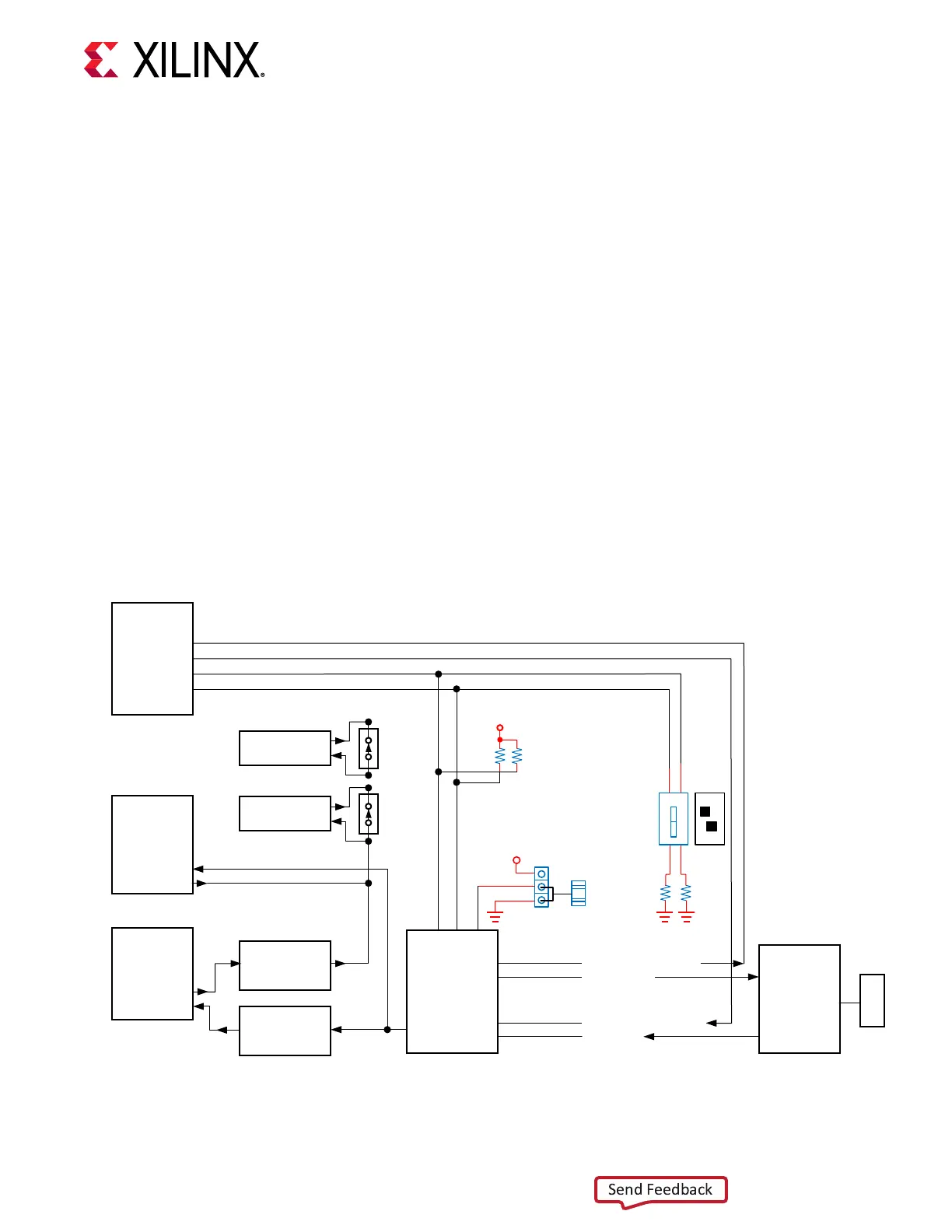
JTAG Chain
[Figure 3, callout 7, 8, and 48]
VCK190 JTAG chain
• J36 2x7 2 mm shrouded, keyed JTAG pod at cable connector
• J207 USB-C connector connected to U20 FT4232HL USB-JTAG bridge
• U125 XCZU4EG System Controller bank 44
Figure 18: JTAG Chain Block Diagram
1
2
XCZU4EG
BANK 44
SYSTEM
CONTROLLER
TDO
TDI
JTAG
2 mm 2X7
Header
TDO
TDI
U125
J36
ACAP U1
BANK 503
Config
JTAG
IF
TDO
TDI
U1
FMC2
J53
TDO
TDI
FMC1
J51
TDO
TDI
N.C.
N.C.
U241 U240
JTAG
TDO
L/S
U16
AB
B-to-A
JTAG
TDI
L/S
U239
AB
A-to-B
JTAG
MUX
U15
1A
2A
1B1
1B2
1B1
2B2
S1 S0 OEn
R88
4.70K
UTIL_3V3
R87
4.70K
SW3
1
ON
ON
2
ON
OFF
SS
01
00
01
CH1
CH2
SYSCTLR
FT4232
JTAG
JTAG
UTIL 3v3
1
2
3
SW3
1
2
R97
499
R98
499
Set SW3
to
“ON OFF”
FT4232HL
UART
BRIDGE
TDO
TDI
U
S
B
J207
SYSCTLR_VERSAL_TDO
FT4232_TDO
SYSCTLR_VERSAL_TDI
FT4232_TDI
U20
X23204-100719
See Versal ACAP Conguraon for informaon on JTAG programming via:
Chapter 3: Board Component Descriptions
UG1366 (v1.0) January 7, 2021 www.xilinx.com
VCK190 Board User Guide 44

 Loading...


