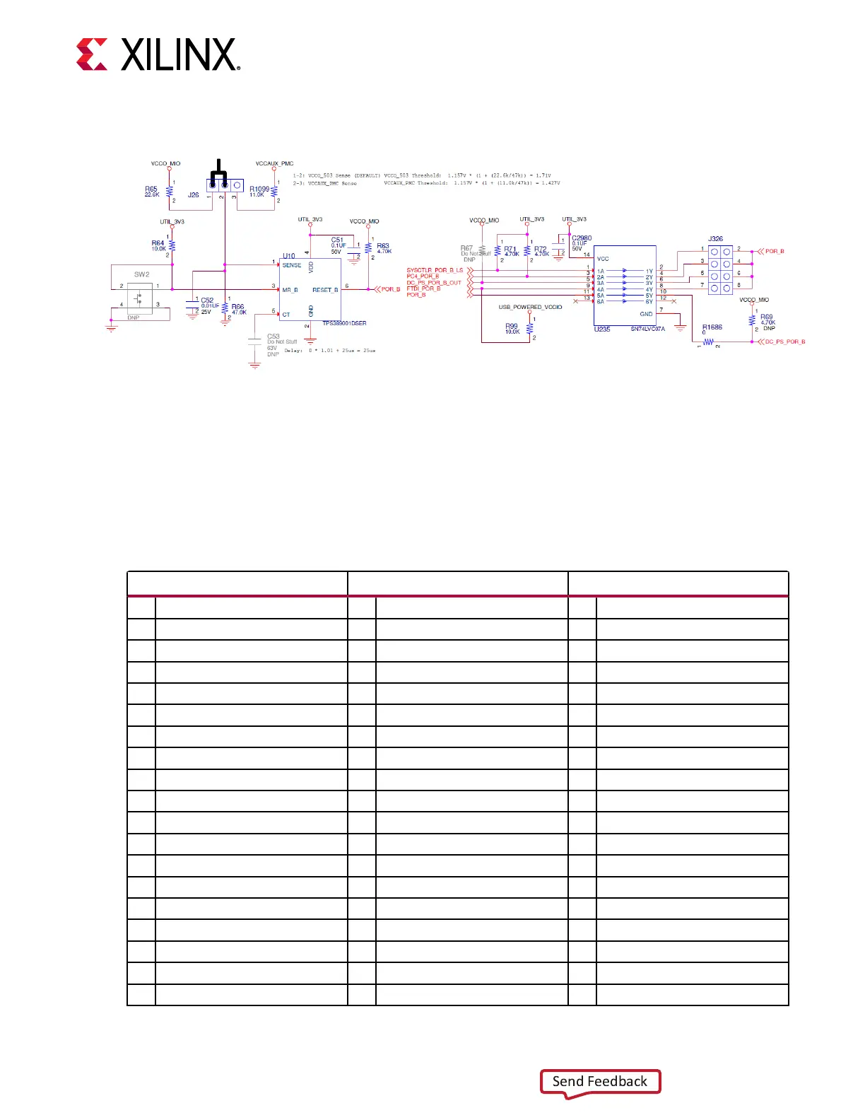
Figure 8: POR_B Reset Circuit
X24949-121420
PMC and LPD MIO
The following table provides MIO peripheral mapping implemented on the VCK190 board. See
the Versal ACAP Technical Reference Manual (AM011) for more informaon on MIO peripheral
mapping. The XCVC1902 ACAP Bank 500, 501, and 502 mappings are listed in the table.
Table 7: MIO Peripheral Mapping
PMC MIO[0:25] Bank 500 PMC MIO[26:51] Bank 501 LPD MIO[0:25] Bank 502
0 MIO CONN. J212 26 SD1 0 GEM0
1 MIO CONN. J212 27 SD1 1 GEM0
2 MIO CONN. J212 28 SD1 2 GEM0
3 MIO CONN. J212 29 SD1 3 GEM0
4 MIO CONN. J212 30 SD1 4 GEM0
5 MIO CONN. J212 31 SD1 5 GEM0
6 MIO CONN. J212 32 SD1 6 GEM0
7 MIO CONN. J212 33 SD1 7 GEM0
8 MIO CONN. J212 34 SD1 8 GEM0
9 MIO CONN. J212 35 SD1 9 GEM0
10 MIO CONN. J212 36 SD1 10 GEM0
11 MIO CONN. J212 37 ZU4_TRIGGER 11 GEM0
12 MIO CONN. J212 38 PCIE_PERST_B 12 GEM1
13 U103.6 USB3320 U99 reset gate 39 PCIE_PWRBRK_B 13 GEM1
14 USB3320 U99 40 CAN1_TXD 14 GEM1
15 USB3320 U99 41 CAN1_RXD 15 GEM1
16 USB3320 U99 42 UART0 16 GEM1
17 USB3320 U99 43 UART0 17 GEM1
18 USB3320 U99 44 I2C1 18 GEM1
Chapter 3: Board Component Descriptions
UG1366 (v1.0) January 7, 2021 www.xilinx.com
VCK190 Board User Guide 28

 Loading...


