Table 7: MIO Peripheral Mapping (cont'd)
PMC MIO[0:25] Bank 500 PMC MIO[26:51] Bank 501 LPD MIO[0:25] Bank 502
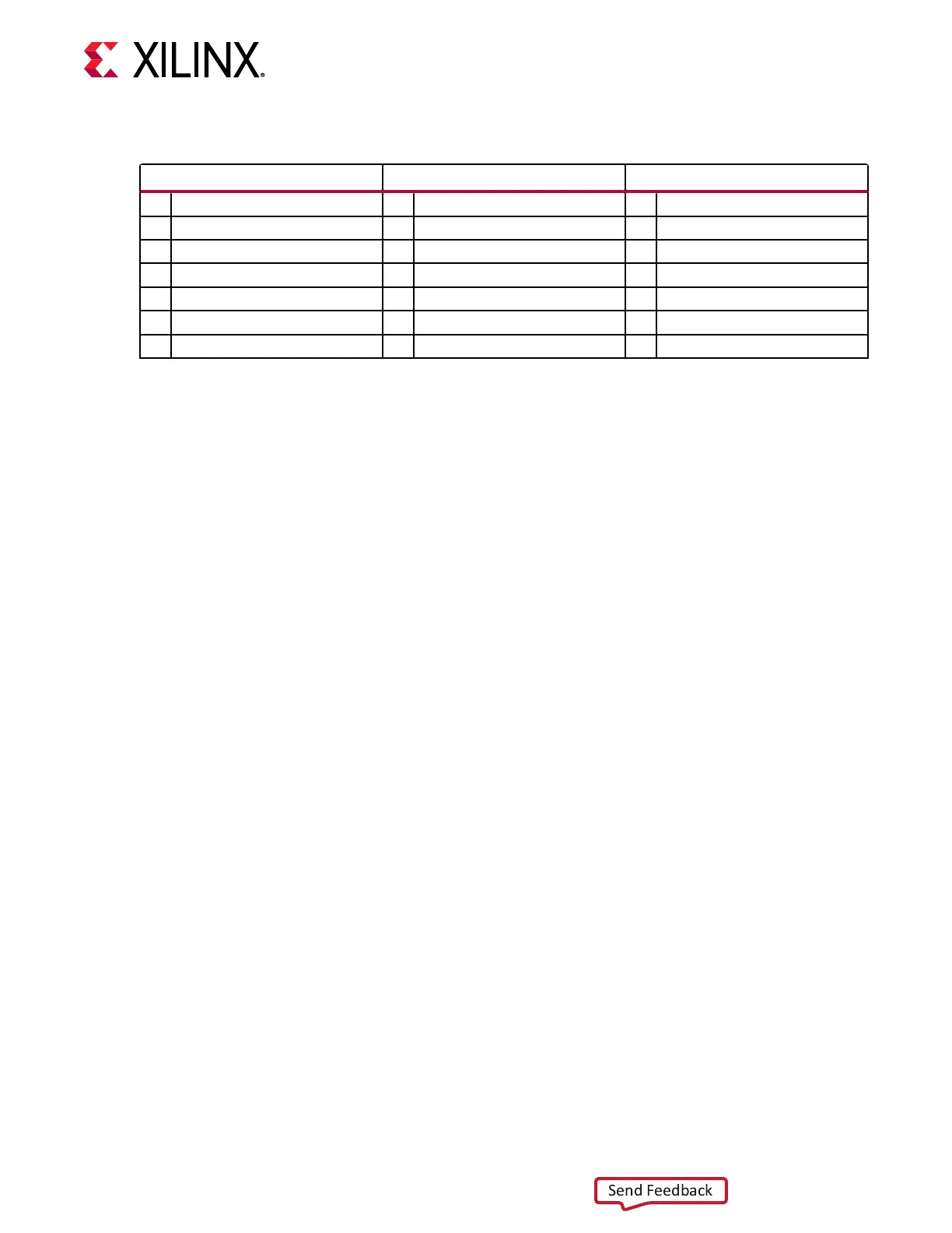
19 USB3320 U99 45 I2C1 19 GEM1
20 USB3320 U99 46 I2C0 20 GEM1
21 USB3320 U99 47 I2C0 21 GEM1
22 USB3320 U99 48 GEM0 22 GEM1
23 USB3320 U99 49 GEM1 23 GEM1
24 USB3320 U99 50 PCIE_WAKE_B 24 GEM0, GEM1
25 USB3320 U99 51 SD1 25 GEM0, GEM1
PMC MIO[0–12] Bank 500: MIO Daughter Card (DC)
Connector J212
[Figure 3, callout 5]
The VCK190 U1 XCVC1902 bank 500 PMC_MIO[0:12] pins are connected to the 240-pin (8 x
30) MIO connector J212. This interface enables high-speed XCVC1902 conguraon using the
X-EBM-01 QSPI external daughter card installed on J212.
The detailed ACAP connecons for the feature described in this secon are documented in the
VCK190 board XDC le, referenced in Appendix B: Xilinx Design Constraints. The XCVC1902
MIO connector J212 pinout is listed in the following gure.
Chapter 3: Board Component Descriptions
UG1366 (v1.0) January 7, 2021 www.xilinx.com
VCK190 Board User Guide 29

 Loading...


