Appendix B
Xilinx Design Constraints
Overview
The Xilinx
®
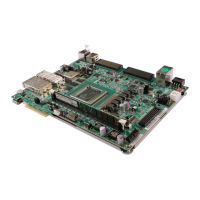
design constraints (XDC) le template for the VCK190 board provides for designs
targeng the VCK190 evaluaon board. Net names in the constraints listed correlate with net
names on the latest VCK190 evaluaon board schemac. Idenfy the appropriate pins and
replace the net names with net names in the user RTL. See the Vivado Design Suite User Guide:
Using Constraints (UG903) for more informaon.
The HSPC FMCP connectors J51 and J53 are connected to ACAP U1 banks powered by the
variable voltage VADJ_FMC. Because dierent FMC cards implement dierent circuitry, the FMC
bank I/O standards must be uniquely dened by each customer.
IMPORTANT!
See the VCK 190 board documentaon ("Board Files" check box) for the XDC le.
Appendix B: Xilinx Design Constraints
UG1366 (v1.0) January 7, 2021 www.xilinx.com
VCK190 Board User Guide 70
 Loading...
