7 Series FPGAs GTP Transceivers User Guide www.xilinx.com 101
UG482 (v1.9) December 19, 2016
TX Buffer Bypass
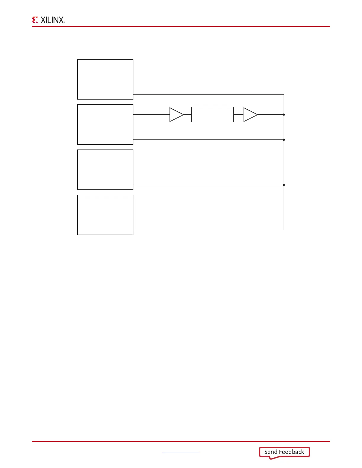
Figure 3-14 shows an example of buffer bypass master versus slave lanes.
These GTP transceiver settings are used to bypass the TX buffer:
• TXBUF_EN = FALSE
• TX_XCLK_SEL = TXUSR
• TXOUTCLKSEL = 3'b011 or 3'b100 to select the GTP transceiver reference clock as the
source of TXOUTCLK
With the GTP transceiver reference clock selected, TXOUTCLK is used as the source of the
TXUSRCLK. The user must ensure that TXOUTCLK and the selected GTP transceiver reference
clock is running and operating at the desired frequency. When the TX buffer is bypassed, the TX
phase alignment procedure must be performed after these events:
• Resetting or powering up the GTP transceiver transmitter
• Resetting or powering up the PLL
• Change of the GTP transceiver reference clock source or frequency
• Change of the TX line rate
X-Ref Target - Figure 3-14
Figure 3-14: TX Buffer Bypass in Multi-Lane Mode Example
UG482_c3_115_020413
BUFG BUFG
GTP TX
Lane 3
Slave
TXUSRCLK
TXUSRCLK2
GTP TX
Lane 2
MMCM / PLL
Master
TXUSRCLK
TXOUTCLK
TXUSRCLK2
GTP TX
Lane 1
Slave
TXUSRCLK
TXUSRCLK2
GTP TX
Lane 0
Slave
TXUSRCLK
TXUSRCLK2
 Loading...