7 Series FPGAs GTP Transceivers User Guide www.xilinx.com 109
UG482 (v1.9) December 19, 2016
TX Fabric Clock Output Control
Serial Clock Divider
Each transmitter PMA module has a D divider that divides down the clock from the PLL for lower
line rate support. This serial clock divider, D, can be set statically for applications with a fixed line
rate or it can be changed dynamically for protocols with multiple line rates.
To use the D divider in fixed line rate applications, the TXOUT_DIV attribute must be set to the
appropriate value, and the TXRATE port needs to be tied to 3'b000. Refer to the Static Setting via
Attribute column in Table 3-23 for details.
To use the D divider in multiple line rate applications, the TXRATE port is used to dynamically
select the D divider value. The TXOUT_DIV attribute and the TXRATE port must select the same
D divider value upon device configuration. After device configuration, the TXRATE is used to
dynamically change the D divider value. Refer to the Dynamic Control via Ports column in
Table 3-23 for details.
The control for the serial divider is shown in Table 3-23. For details about the line rate range per
speed grade, refer to the 7 series FPGAs documentation page
for the appropriate data sheet.
Parallel Clock Divider and Selector
The parallel clock outputs from the TX clock divider control block can be used as a fabric logic
clock, depending on the line rate requirement.
The recommended clock for the fabric is the TXOUTCLK from one of the GTP transceivers. It is
also possible to bring the MGTREFCLK directly to the FPGA logic and use as the fabric clock.
TXOUTCLK is preferred for general applications as it has an output delay control used for
applications that bypass the TX buffer for output lane deskewing or constant datapath delay. Refer
to TX Pattern Generator, page 103 for more details.
The TXOUTCLKSEL port controls the input selector and allows these clocks to be output via the
TXOUTCLK port:
• TXOUTCLKSEL = 3'b001: The TXOUTCLKPCS path is not recommended for use because
it incurs extra delay from the PCS block.
• TXOUTCLKSEL = 3'b010: TXOUTCLKPMA is the divided down PLL clock after the TX
phase interpolator and is used by the TX PCS block. This clock is interrupted when the PLL is
reset by one of the related reset signals.
• TXOUTCLKSEL = 3'b011 or 3'b100: TXPLLREFCLK_DIV1 or
TXPLLREFCLK_DIV2 is the input reference clock to PLL0 or PLL1, depending on the
TXSYSCLKSEL[1] setting. TXPLLREFCLK is the recommended clock for general usage and
is required for the TX buffer bypass mode.
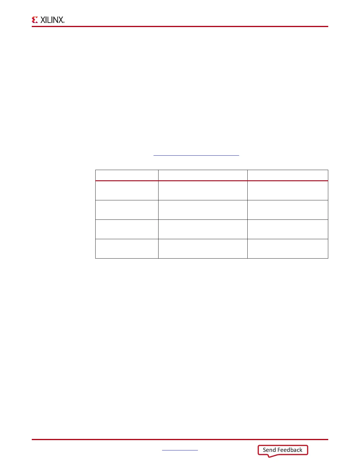
Table 3-23: TX PLL Output Divider Setting
D Divider Value Static Setting via Attribute Dynamic Control via Ports
1
TXOUT_DIV = 1
TXRATE = 3'b000
TXOUT_DIV = Ignored
TXRATE = 3'b001
2
TXOUT_DIV = 2
TXRATE = 3'b000
TXOUT_DIV = Ignored
TXRATE = 3'b010
4
TXOUT_DIV = 4
TXRATE = 3'b000
TXOUT_DIV = Ignored
TXRATE = 3'b011
8
TXOUT_DIV = 8
TXRATE = 3'b000
TXOUT_DIV = Ignored
TXRATE = 3'b100
 Loading...