74 ADV200 • Functions description and parameters list
Menu PAR Description UM Type FB BIT Def Min Max Acc Mod
15.1 1800 Analog out 1 src LINK 16/32 6000 0 16384 RW FVS
15.2 1802 Analog out 2 src LINK 16/32 6000 0 16384 RW FVS
Selection of the origin (source) of the signals that can be placed as variables on the analog outputs. The func-
tions that can be assigned to the analog outputs are listed in the “L_ANOUT” selection list.
Menu PAR Description UM Type FB BIT Def Min Max Acc Mod
15.3 1808 Analog out 1 scale FLOAT 1.0 -10.0 10.0 RW FVS
15.4 1810 Analog out 2 scale FLOAT 1.0 -10.0 10.0 RW FVS
Parameter for setting a multiplier factor of the signal of the relative analog output. It can be used to amplify or
reduce the input value of the relative analog output block.
1
2
3
+10V
-10V
0V
Internal V
1
2
3
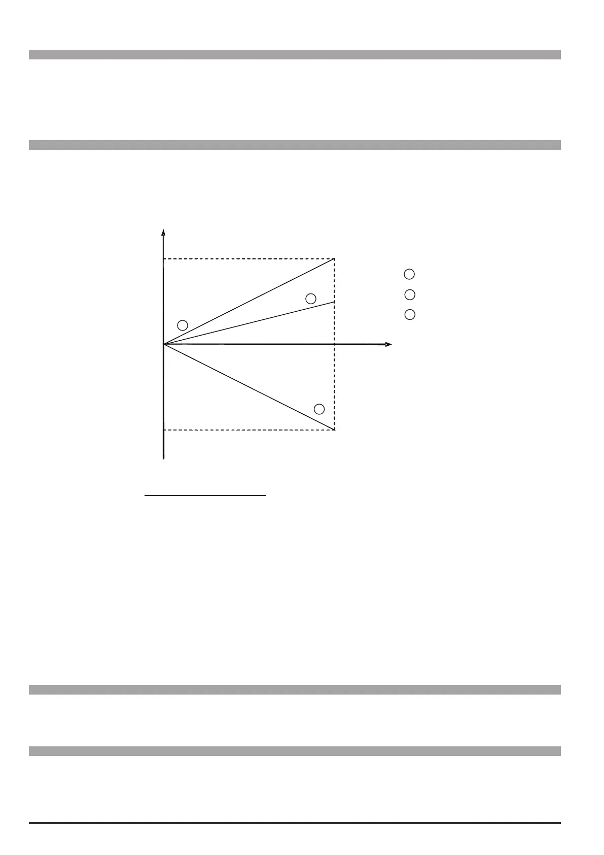
Par. 1808 (1810) =1
Par. 1808 (1810) =
Par. 1808 (1810)=-1
Stp Var x par. 1808 (1810)
Vout = 10 x ( )
FS Var
where:
Vout output voltage on the card terminals.
Stp Var actual value of the variable (variable unit)
SF Var full scale of the variable (variable unit)
Example of calculation of scale factor Analog out x scale
To display the drive speed, use an analog instrument with eld of measurement from 0...2V. This means that, to
display the speed of the drive, a voltage of 2V on the analog output of the drive must correspond to the maxi-
mum speed. With a scale factor equal to 1 a voltage of 10V would correspond to the maximum speed.
With a scale factor equal to 0.2 = 2V/10V a voltage of 2V would correspond to the maximum speed.
Menu PAR Description UM Type FB BIT Def Min Max Acc Mod
15.5 1816 Analog out 1 mon cnt INT16 0 0 0 ER FVS
The value of the actual voltage present on analog output 1 is displayed.
Menu PAR Description UM Type FB BIT Def Min Max Acc Mod
15.6 1818 Analog out 2 mon cnt INT16 0 0 0 ER FVS
The value of the actual voltage or current present on analog output 2 is displayed.
 Loading...