6 3
KEB COMBIVERT F5
18
Name: Basis
28.01.03
Chapter Section Page Date
© KEB Antriebstechnik, 2002
All rights reserved
Functional Description Digital In- and Outputs
6.3.22 Inversion of Out-
puts (do.42)
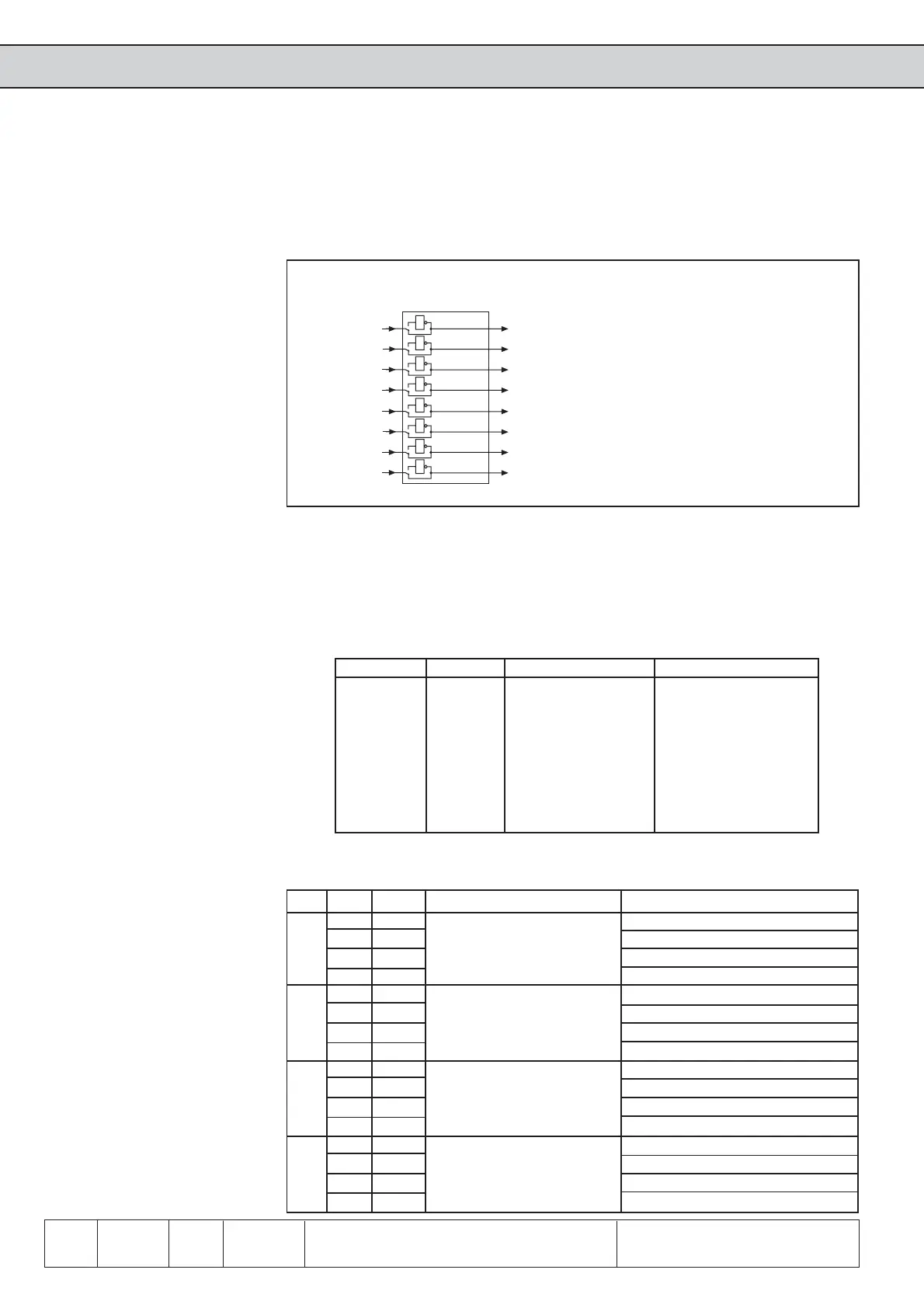
As shown in Fig. 6.3.21, with parameter do.42 the outputs can be once again inverted
after the linking. The parameter is bit-coded, i.e. according to following table the value
belonging to this output must be entered. If several outputs shall be inverted the sum
is to be formed
6.3.23 Output Terminal
Status (ru.25)
Parameter ru.25 indicates the logic condition of the digital outputs after the allocation
by do.51. Parameter ru.80 indicates the logic condition before the allocation. It is
irrelevant whether the output is set due to conditions or by inverting. If an output is set
the appropriate decimal value, according to the table below, is output. If several outputs
are set, then the sum of the decimal values is output.
1
1
1
1
do.42
Bit 0
Bit 1
Bit 2
Bit 3
Bit 4
Bit 5
Bit 6
Bit 7
1
2
4
8
16
32
64
128
1
1
1
1
do.41
Terminal Name Function
X2A.18 O1 Transistor output
X2A.19 O2 Transistor output
X2A.24...26 R1 Relay output
X2A.27...29 R2 Relay output
- OA Internal output
- OB Internal output
- OC Internal output
- OD Internal output
Fig. 6.3.21 Inverting the outputs
Terminal Name Function Decimal values ru.25
X2A.18 O1 Transistor output 1
X2A.19 O2 Transistor output 2
X2A.24...26 R1 Relay output 4
X2A.27...29 R2 Relay output 8
- OA Internal output 16
- OB Internal output 32
- OC Internal output 64
- OD Internal output 128
6.3.24 Hardware output
allocation (do.51)
With do.51 the output signals are assigned to the output terminals O1, O2, R1 and R2.
The assignment is done according to following table:
Bit Value Signal Output Default
0 + 1 0 O1 x
1 O2 O1 (terminal X2A.18)
2R1
3R2
2+3 0 O1
4 O2 O2 (terminal X2A.19) x
8R1
16 R2
4+5 0 O1
16 O2 R1 (terminal X2A.24...26)
32 R1 x
48 R2
6+7 0 O1
16 O2 R2 (terminal X2A.27...29)
32 R1
48 R2 x
 Loading...