Theory of Operation
6-7
6.4.2 Switch card interface
The simplified block diagram of the backplane (Figure
6-5) shows two different switch card interfaces. One of
these interfaces supports the Model 7052-7169 series
switch cards while the other supports the Model 7011-
7013 series switch cards.
The Model 7052-7169 switch card interface connectors
J2000A/J2000B provide +6V, 12 sink drive lines, and a
3-line serial bus to support an additional 8 drive lines
located on an installed switch card. This interface sup-
ports all Model 705 and 706 cards.
The Model 7011-7013 switch card interface connectors
J2001A/J2001B provide +6V, +14.6V, +5V, a 4-line serial
bus for relay driver communication, a 2-line serial bus
for card identification, a 3-line serial bus for I/O data
communication, and four 3-line analog bus expansions
between slot 1 and slot 2. The serial bus communica-
tion supports 40 drive lines or 40 I/O lines on each in-
stalled switch card. This 32-pin DIN connector
supports the Model 7011-7013 switch cards.
6.4.3 ID data circuits
Upon power-up, the mainframe reads card identifica-
tion from any cards plugged into the mainframe. This
ID data includes such information as card ID, hard-
ware settling times, and relay configuration informa-
tion.
ID data is contained within an EEPROM which is locat-
ed on the relay card. The system performs the follow-
ing sequence of operations at power-up in order to
read the information:
1. The IDDATA line (pin 6 of the EEPROM located on
the relay card) is set low while the IDCLK line (pin
5) is held high. This action initiates a start com-
mand for the ROM located on the relay card to
transmit data serially to the mainframe (see Figure
6-6).
2. The mainframe sends the ROM address location to
be read over the IDDATA line. The ROM then
transmits an acknowledge signal back to the main-
frame, and then transmits data at that location
back to the mainframe (refer back to Figure 6-5).
3. The mainframe then transmits an acknowledge
signal indicating that it requires more data. The
ROM on the relay card will then sequentially trans-
mit data after each acknowledge signal it receives.
4. Once all data are received, the mainframe sends a
stop command. The stop command consists of a
low-to-high transition of the IDDATA line while
the IDCLK line is held high (see Figure 6-7).
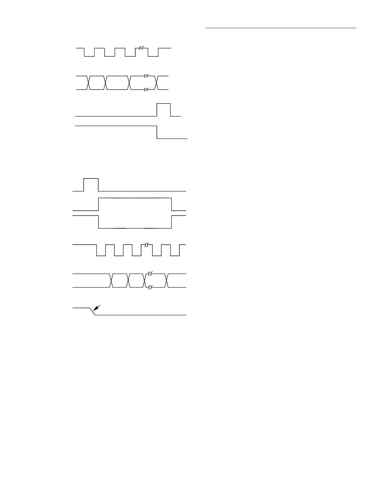
Figure 6-4
Timing diagram
backplane interface WRITE
Relay CLK
Relay Data
Strobe
Enable (for first
write only)
A. Backplane Interface for Write Timing
B. Backplane Interface for Read
Timing
Strobe
R/W
CS
Relay CLK
I/O Data
Enable
Same edge as
strobe for first read.
Artisan Scientific - Quality Instrumentation ... Guaranteed | (888) 88-SOURCE | www.artisan-scientific.com
 Loading...