Theory of Operation
6-9
6.4.4 Relay control
Card relays are controlled by serial data transmitted
via the relay DATA line. Five bytes for each card are
shifted in serial fashion into latches located in the card
and backplane relay driver ICs. The serial data is
clocked in by the CLK line. As data overflows one reg-
ister, it is fed out the Q’s line of the register down the
chain.
Once all five bytes have been shifted into the drivers,
the STROBE line is set high to latch the relay informa-
tion into the Q outputs of the relay drivers. The appro-
priate relays are also energized (assuming the driver
outputs are enabled, as discussed below). Note that a
relay driver output goes low to energize the corre-
sponding relay.
6.4.5 Power-on safeguard
A power-on safeguard circuit, consisting of U114 (a D-
type flip-flop) and associated components, ensures
that relays do not randomly energize on power-up and
power-down. This circuit disables all relays to an open
condition during power-up and power-down periods.
The PRESET line on the D-type flip-flop is controlled
via the SYSRST line by the 68302 microprocessor, while
the CLK line is controlled by a VIA port line from the
68302. The Q output of the flip-flop drives each switch
card relay driver IC enable pin (U100-U104, pin 8).
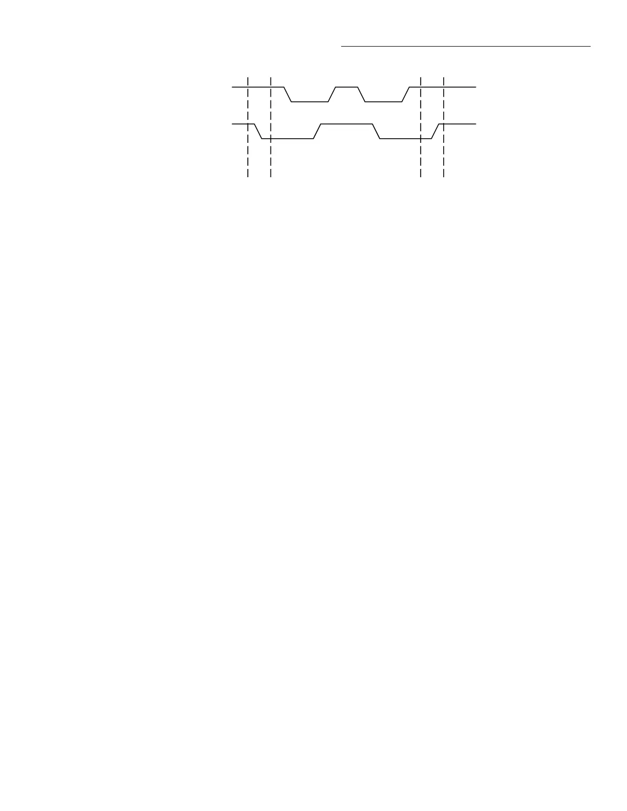
Figure 6-7
Start and stop sequences
ID CLK
ID DATA
Start Bit Stop Bit
When the 68302 microprocessor is in the RESET mode,
the flip-flop PRESET line is held low, and the Q output
immediately goes high, disabling all relays (the relay
driver IC enable pins are high, disabling the relays).
After the reset condition elapses (requiring approxi-
mately 200msec), PRESET goes high while the Q out-
put stays high. With the first valid STROBE pulse, a
low logic level is clocked into the D-type flip-flop, set-
ting the Q output low and simultaneously enabling all
relay drivers. Note that the Q output stays low (en-
abling the relay drivers), until the 68302 processor goes
into a reset condition.
6.4.6 Display board circuitry
A block diagram of the display board is shown in Fig-
ure 6-8. Major components include the display micro-
controller, the dot and grid drivers, the vacuum
fluorescent display (VFD), and the key matrix.
The 68HC705 is the display microcontroller that con-
trols the VFD and interprets key data. The microcon-
troller has four peripheral I/O ports, which are used
for the various control and read functions. Display
data is serially transmitted to the microcontroller from
the digital board via the TXB line to the microcontroller
PD0 terminal. In a similar manner, key data is serially
sent back to the digital board through the RXB line via
PD1.
Note that the 4MHz display clock is generated on the
digital board.
Artisan Scientific - Quality Instrumentation ... Guaranteed | (888) 88-SOURCE | www.artisan-scientific.com
 Loading...