Clock Generator Module (CGM)
CGM Registers
MC68HC908AB32 — Rev. 1.0 Technical Data
MOTOROLA Clock Generator Module (CGM) 149
NOTE:
The multiplier select bits have built-in protection that prevents them from
being written when the PLL is on (PLLON = 1).
VRS[7:4] — VCO Range Select Bits
These read/write bits control the hardware center-of-range linear
multiplier L, which controls the hardware center-of-range frequency
f
VRS
. (See 9.4.2.1 PLL Circuits, 9.4.2.4 Programming the PLL, and
9.6.1 PLL Control Register (PCTL)). VRS[7:4] cannot be written
when the PLLON bit in the PLL control register (PCTL) is set. (See
9.4.2.5 Special Programming Exceptions). A value of $0 in the
VCO range select bits disables the PLL and clears the BCS bit in the
PCTL. (See 9.4.3 Base Clock Selector Circuit and 9.4.2.5 Special
Programming Exceptions for more information). Reset initializes
the bits to $6 to give a default range multiply value of 6.
NOTE:
The VCO range select bits have built-in protection that prevents them
from being written when the PLL is on (PLLON = 1) and prevents
selection of the VCO clock as the source of the base clock (BCS = 1) if
the VCO range select bits are all clear.
The VCO range select bits must be programmed correctly. Incorrect
programming may result in failure of the PLL to achieve lock.
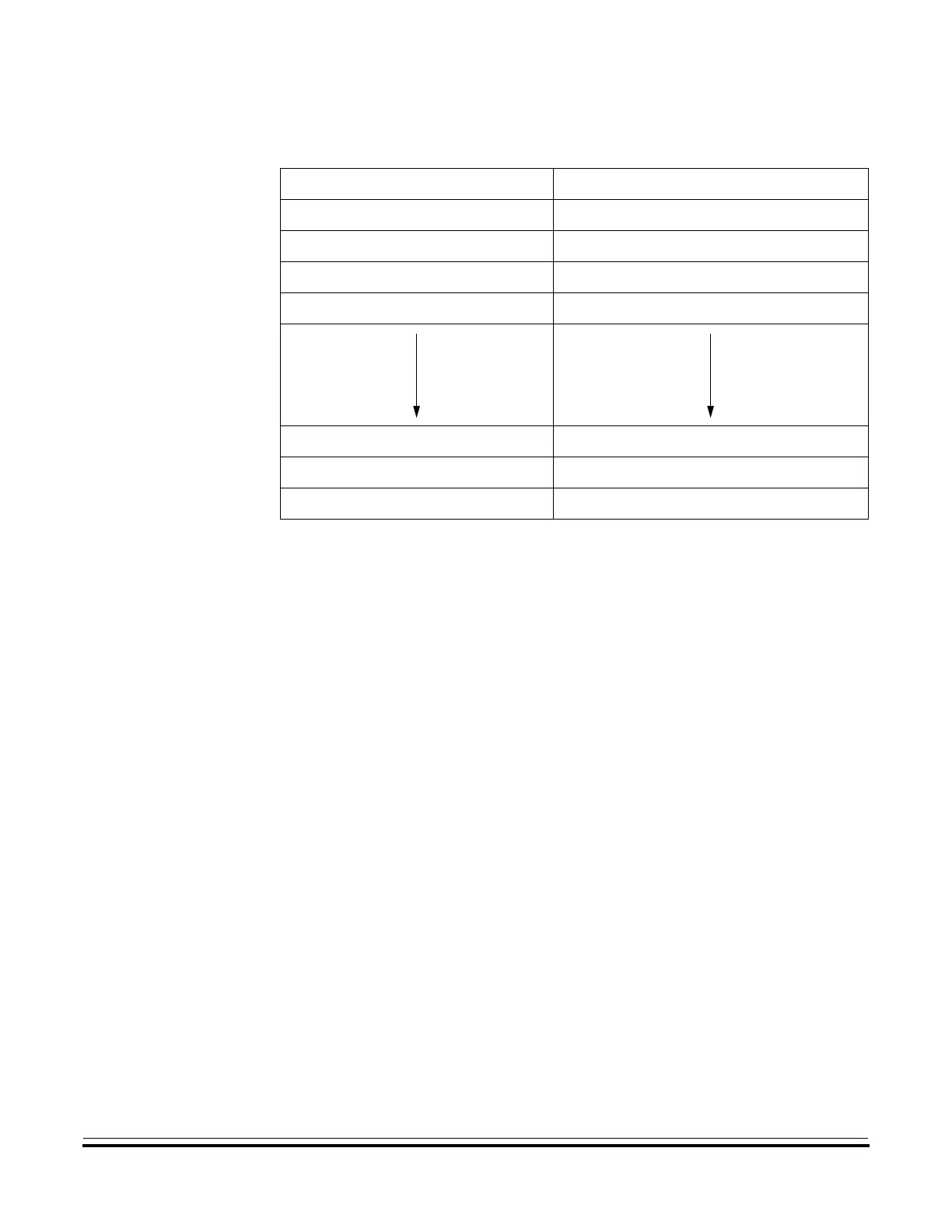
Table 9-1. VCO Frequency Multiplier (N) Selection
MUL7:MUL6:MUL5:MUL4 VCO Frequency Multiplier (N)
0000 1
0001 1
0010 2
0011 3
1101 13
1110 14
1111 15
 Loading...


