Serial Peripheral Interface Module (SPI)
Transmission Formats
MC68HC908AB32 — Rev. 1.0 Technical Data
MOTOROLA Serial Peripheral Interface Module (SPI) 287
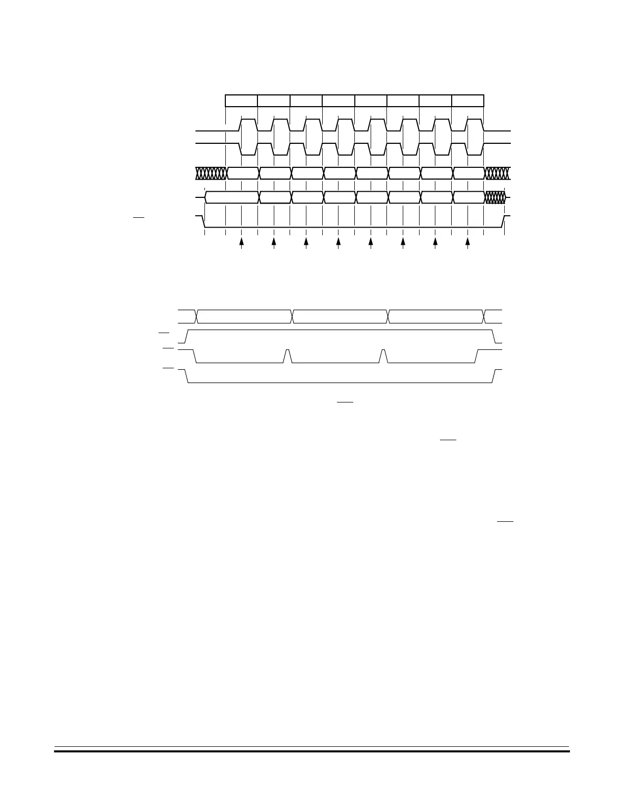
Figure 16-4. Transmission Format (CPHA = 0)
Figure 16-5. CPHA/SS Timing
When CPHA = 0 for a slave, the falling edge of SS
indicates the
beginning of the transmission. This causes the SPI to leave its idle state
and begin driving the MISO pin with the MSB of its data. Once the
transmission begins, no new data is allowed into the shift register from
the transmit data register. Therefore, the SPI data register of the slave
must be loaded with transmit data before the falling edge of SS
. Any data
written after the falling edge is stored in the transmit data register and
transferred to the shift register after the current transmission.
BIT 6 BIT 5 BIT 4 BIT 3 BIT 2 BIT 1 LSB
MSB
BIT 6 BIT 5 BIT 4 BIT 3 BIT 2 BIT 1 LSB
MSB
12345678
SPSCK CYCLE #
FOR REFERENCE
SPSCK; CPOL = 0
SPSCK; CPOL =1
MOSI
FROM MASTER
MISO
FROM SLAVE
SS
; TO SLAVE
CAPTURE STROBE
BYTE 1 BYTE 3
MISO/MOSI
BYTE 2
MASTER SS
SLAVE SS
CPHA = 0
SLAVE SS
CPHA = 1
 Loading...


