Analog-to-Digital Converter (ADC)
Functional Description
MC68HC908AB32 — Rev. 1.0 Technical Data
MOTOROLA Analog-to-Digital Converter (ADC) 231
14.4 Functional Description
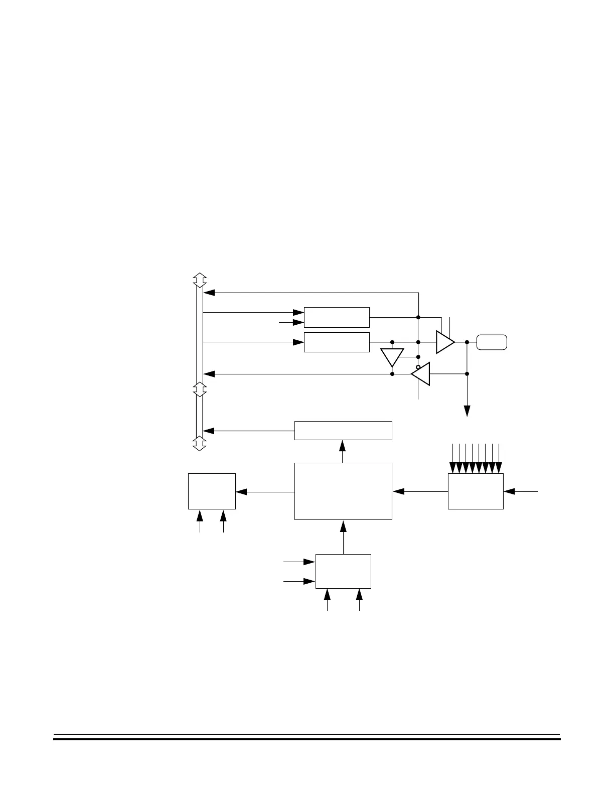
The ADC provides eight pins for sampling external sources at pins
PTB7/ATD7–PTB0/ATD0. An analog multiplexer allows the single ADC
converter to select one of eight ADC channels as ADC voltage in
(V
ADIN
). V
ADIN
is converted by the successive approximation
register-based analog-to-digital converter. When the conversion is
completed, ADC places the result in the ADC data register and sets a
flag or generates an interrupt. (See Figure 14-2.)
Figure 14-2. ADC Block Diagram
INTERNAL
DATA BUS
READ DDRBx
WRITE DDRBx
RESET
WRITE PTBx
READ PTBx
PTBx
DDRBx
PTBx
INTERRUPT
LOGIC
CHANNEL
SELECT
ADC
CLOCK
GENERATOR
CONVERSION
COMPLETE
ADC
(V
ADIN
)
ADC CLOCK
CGMXCLK
BUS CLOCK
ADCH[4:0]
ADC DATA REGISTER
AIEN COCO
DISABLE
DISABLE
ADC CHANNEL x
ADIV[2:0] ADICLK
VOLTAGE IN
ADC I/P CHANNELS
 Loading...


