Input/Output (I/O) Ports
Technical Data MC68HC908AB32 — Rev. 1.0
334 Input/Output (I/O) Ports MOTOROLA
DDRG[2:0] — Data Direction Register G Bits
These read/write bits control port G data direction. Reset clears
DDRG[2:0], configuring all port G pins as inputs.
1 = Corresponding port G pin configured as output
0 = Corresponding port G pin configured as input
NOTE:
Avoid glitches on port G pins by writing to the port G data register before
changing data direction register G bits from 0 to 1. Figure 17-24 shows
the port G I/O logic.
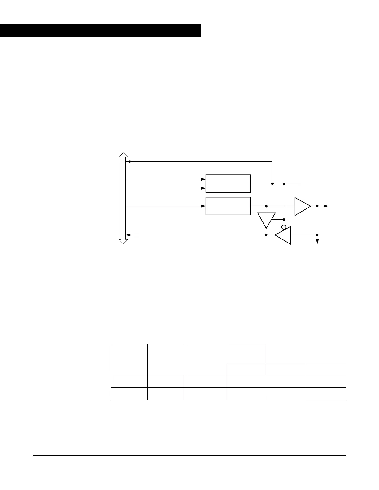
Figure 17-24. Port G I/O Circuit
When DDRGx is a logic 1, reading address $000A reads the PTGx data
latch. When DDRGx is a logic 0, reading address $000A reads the
voltage level on the pin. The data latch can always be written, regardless
of the state of its data direction bit.
Table 17-6 summarizes the operation of the port G pins.
Table 17-8. Port G Pin Functions
DDRG
Bit
PTG Bit
I/O Pin
Mode
Accesses
to DDRG
Accesses to PTG
Read/Write Read Write
0X
(1)
Notes:
1. X = don’t care.
Input, Hi-Z
(2)
2. Hi-Z = high impedance.
DDRG[2:0] Pin PTG[2:0]
(3)
3. Writing affects data register, but does not affect the input.
1 X Output DDRG[2:0] PTG[2:0] PTG[2:0]
READ DDRG ($000E)
WRITE DDRG ($000E)
RESET
WRITE PTG ($000A)
READ PTG ($000A)
PTGx
DDRGx
PTGx
INTERNAL DATA BUS
KBI
 Loading...


