Timer Interface Module A (TIMA)
I/O Registers
MC68HC908AB32 — Rev. 1.0 Technical Data
MOTOROLA Timer Interface Module A (TIMA) 191
NOTE:
Before enabling a TIMA channel register for input capture operation,
make sure that the TACHx pin is stable for at least two bus clocks.
TOVx — Toggle-On-Overflow Bit
When channel x is an output compare channel, this read/write bit
controls the behavior of the channel x output when the TIMA counter
overflows. When channel x is an input capture channel, TOVx has no
effect. Reset clears the TOVx bit.
1 = Channel x pin toggles on TIMA counter overflow.
0 = Channel x pin does not toggle on TIMA counter overflow.
NOTE:
When TOVx is set, a TIMA counter overflow takes precedence over a
channel x output compare if both occur at the same time.
CHxMAX — Channel x Maximum Duty Cycle Bit
When the TOVx bit is at logic zero, setting the CHxMAX bit forces the
duty cycle of buffered and unbuffered PWM signals to 100%. As
Figure 11-13 shows, the CHxMAX bit takes effect in the cycle after it
is set or cleared. The output stays at the 100% duty cycle level until
the cycle after CHxMAX is cleared.
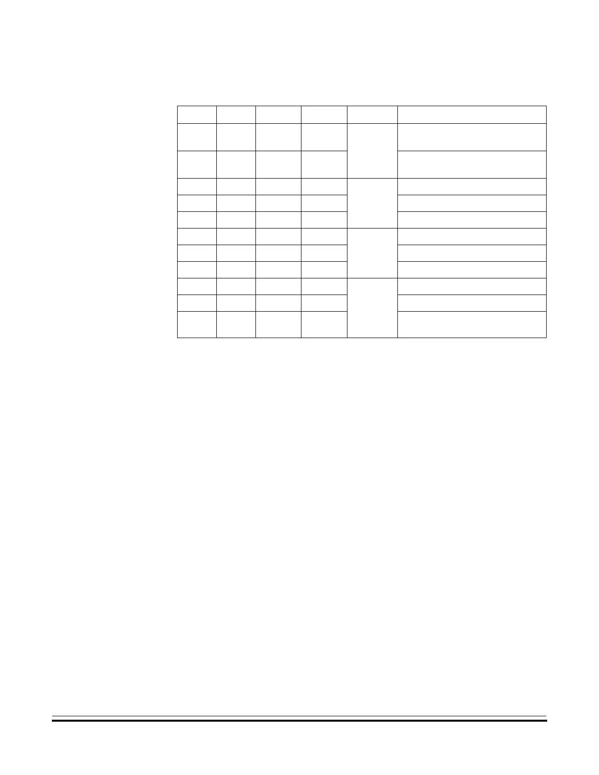
Table 11-3. Mode, Edge, and Level Selection
MSxB MSxA ELSxB ELSxA Mode Configuration
X0 0 0
Output
Preset
Pin under Port Control;
Initial Output Level High
X1 0 0
Pin under Port Control;
Initial Output Level Low
00 0 1
Input
Capture
Capture on Rising Edge Only
0 0 1 0 Capture on Falling Edge Only
0 0 1 1 Capture on Rising or Falling Edge
01 0 1
Output
Compare
or PWM
Toggle Output on Compare
0 1 1 0 Clear Output on Compare
0 1 1 1 Set Output on Compare
1 X 0 1 Buffered
Output
Compare or
Buffered
PWM
Toggle Output on Compare
1 X 1 0 Clear Output on Compare
1 X 1 1 Set Output on Compare
 Loading...


