Serial Peripheral Interface Module (SPI)
Pin Name Conventions and I/O Register Addresses
MC68HC908AB32 — Rev. 1.0 Technical Data
MOTOROLA Serial Peripheral Interface Module (SPI) 281
16.4 Pin Name Conventions and I/O Register Addresses
The text that follows describes the SPI. The SPI I/O pin names are SS
(slave select), SPSCK (SPI serial clock), CGND (clock ground), MOSI
(master out slave in), and MISO (master in/slave out). The SPI shares
four I/O pins with four parallel I/O ports.
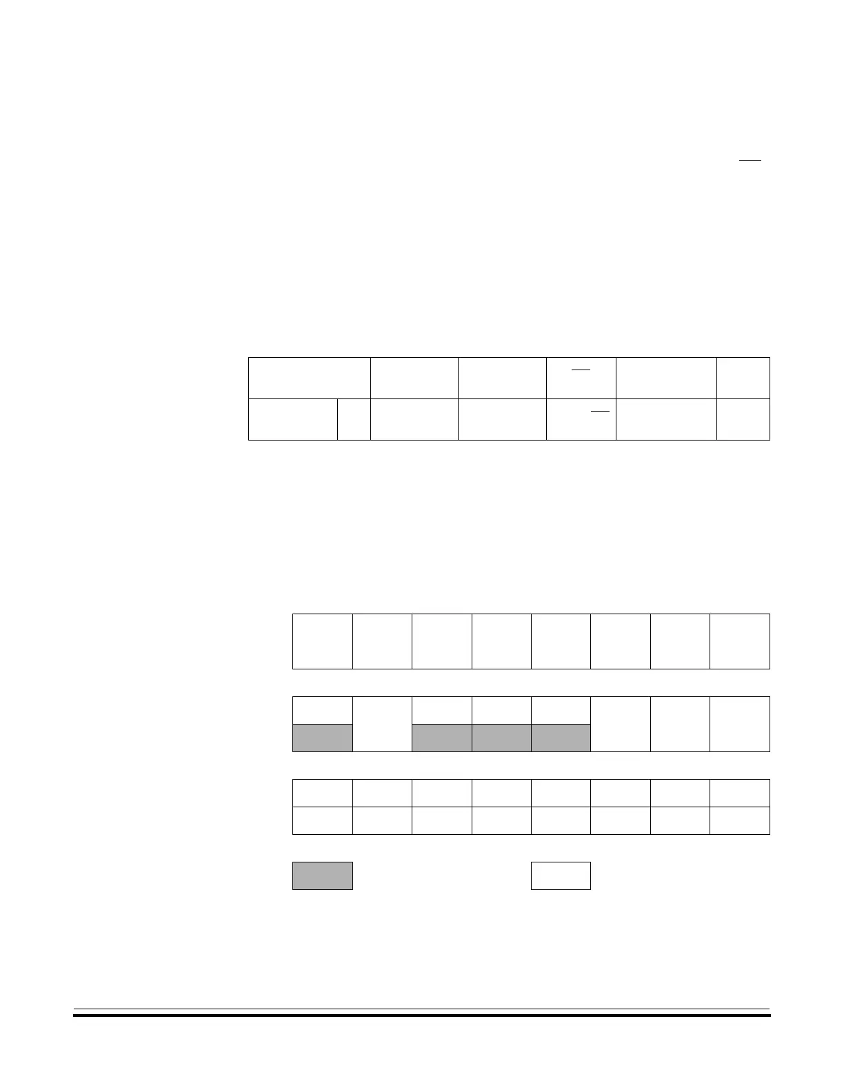
The full names of the SPI I/O pins are shown in Table 16-1. The generic
pin names appear in the text that follows.
16.5 Functional Description
Figure 16-1 summarizes the SPI I/O registers and Figure 16-2 shows
the structure of the SPI module.
Table 16-1. Pin Name Conventions
SPI Generic
Pin Names:
MISO MOSI SS SPSCK CGND
Full SPI
Pin Names:
SPI PTE5/MISO PTE6/MOSI PTE4/SS PTE7/SPSCK
V
SS
Addr. Register Name Bit 7 654321Bit 0
$0010
SPI Control Register
(SPCR)
Read:
SPRIE R SPMSTR CPOL CPHA SPWOM SPE SPTIE
Write:
Reset: 00101000
$0011
SPI Status and Control
Register (SPSCR)
Read: SPRF
ERRIE
OVRF MODF SPTE
MODFEN SPR1 SPR0
Write:
Reset: 00001000
$0012
SPI Data Register
(SPDR)
Read: R7 R6 R5 R4 R3 R2 R1 R0
Write: T7 T6 T5 T4 T3 T2 T1 T0
Reset: Unaffected by reset
= Unimplemented R = Reserved
Figure 16-1. SPI I/O Register Summary
 Loading...


