Input/Output (I/O) Ports
Port F
MC68HC908AB32 — Rev. 1.0 Technical Data
MOTOROLA Input/Output (I/O) Ports 329
When DDREx is a logic 1, reading address $0008 reads the PTEx data
latch. When DDREx is a logic 0, reading address $0008 reads the
voltage level on the pin. The data latch can always be written, regardless
of the state of its data direction bit.
Table 17-6 summarizes the operation of the port E pins.
17.8 Port F
Port F is an 8-bit special function port that shares six of its pins with the
timer interface modules (TIMA and TIMB).
17.8.1 Port F Data Register (PTF)
The port F data register contains a data latch for each of the eight port F
pins.
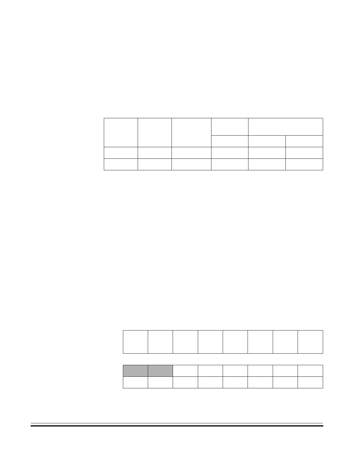
Table 17-6. Port E Pin Functions
DDRE
Bit
PTE Bit
I/O Pin
Mode
Accesses
to DDRE
Accesses to PTE
Read/Write Read Write
0X
(1)
Notes:
1. X = don’t care.
Input, Hi-Z
(2)
2. Hi-Z = high impedance.
DDRE[7:0] Pin PTE[7:0]
(3)
3. Writing affects data register, but does not affect the input.
1 X Output DDRE[7:0] PTE[7:0] PTE[7:0]
Address: $0009
Bit 7 654321Bit 0
Read:
PTF7 PTF6 PTF5 PTF4 PTF3 PTF2 PTF1 PTF0
Write:
Reset: Unaffected by reset
Alternative Function: TBCH1 TBCH0 TBCH3 TBCH2 TACH3 TACH2
Additional Function:
Input pullup Input pullup Input pullup Input pullup Input pullup Input pullup Input pullup Input pullup
Figure 17-18. Port F Data Register (PTF)
 Loading...


