Input/Output (I/O) Ports
Technical Data MC68HC908AB32 — Rev. 1.0
320 Input/Output (I/O) Ports MOTOROLA
When DDRBx is a logic 1, reading address $0001 reads the PTBx data
latch. When DDRBx is a logic 0, reading address $0001 reads the
voltage level on the pin. The data latch can always be written, regardless
of the state of its data direction bit.
Table 17-3 summarizes the operation of the port B pins.
17.5 Port C
Port C is a 6-bit general-purpose bidirectional I/O port. PTC2 pin can be
configured as an output pin for the system MCLK clock.
17.5.1 Port C Data Register (PTC)
The port C data register contains a data latch for each of the six port C
pins.
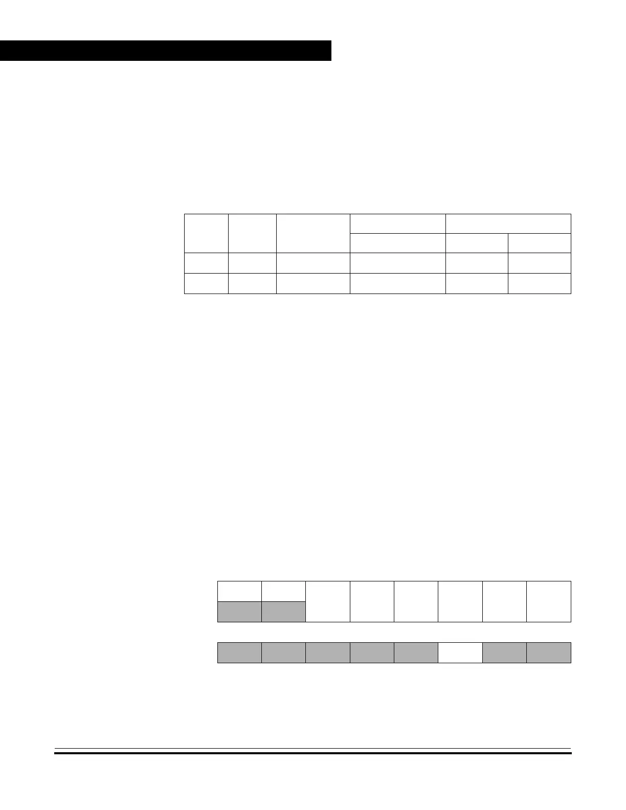
Table 17-3. Port B Pin Functions
DDRB
Bit
PTB Bit I/O Pin Mode
Accesses to DDRB Accesses to PTB
Read/Write Read Write
0X
(1)
Notes:
1. X = don’t care.
Input, Hi-Z
(2)
2. Hi-Z = high impedance.
DDRB[7:0] Pin PTB[7:0]
(3)
3. Writing affects data register, but does not affect input.
1 X Output DDRB[7:0] PTB[7:0] PTB[7:0]
Address: $0002
Bit 7 654321Bit 0
Read: 0 0
PTC5 PTC4 PTC3 PTC2 PTC1 PTC0
Write:
Reset: Unaffected by reset
Alternative Function: MCLK
Figure 17-8. Port C Data Register (PTC)
 Loading...


