Low-Voltage Inhibit (LVI)
Technical Data MC68HC908AB32 — Rev. 1.0
360 Low-Voltage Inhibit (LVI) MOTOROLA
21.4 Functional Description
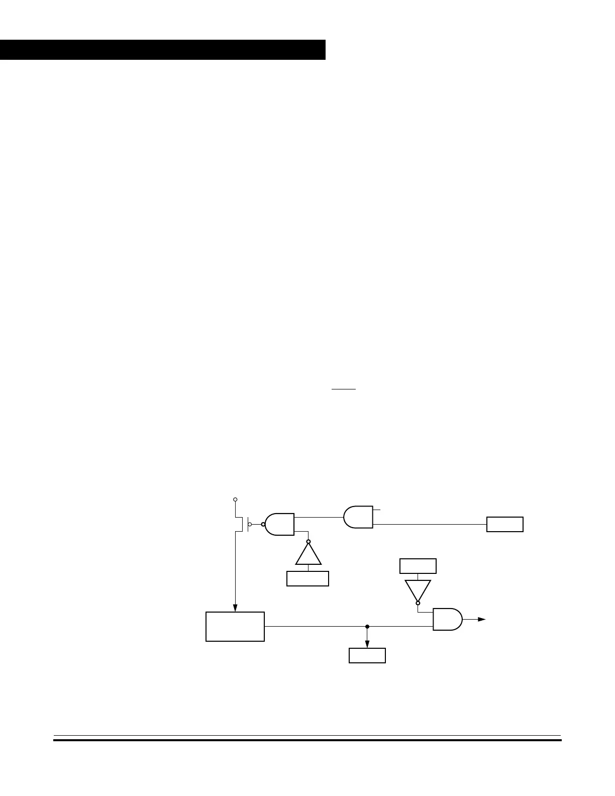
Figure 21-1 shows the structure of the LVI module. The LVI is enabled
out of reset. The LVI module contains a bandgap reference circuit and
comparator. The LVI power bit, LVIPWRD, enables the LVI to monitor
V
DD
voltage. The LVI reset bit, LVIRSTD, enables the LVI module to
generate a reset when V
DD
falls below a voltage, LVI
TRIPF
, and remains
at or below that level for 9 or more consecutive CPU cycles. Setting the
LVI enable in stop mode bit, LVISTOP, enables the LVI to operate in stop
mode.
LVISTOP, LVIPWRD, and LVIRSTD are in the configuration register 1
(CONFIG1). See Section 6. Configuration Register (CONFIG) for
details of the LVI’s configuration bits. Once an LVI reset occurs, the
MCU remains in reset until V
DD
rises above a voltage, LVI
TRIPR
, which
causes the MCU to exit reset. See 8.4.2.5 Low-Voltage Inhibit (LVI)
Reset for details of the interaction between the SIM and the LVI. The
output of the comparator controls the state of the LVIOUT flag in the LVI
status register (LVISR).
An LVI reset also drives the RST
pin low to provide low-voltage
protection to external peripheral devices.
NOTE:
Where LVI trip falling voltage LVI
TRIPF
= V
LVII
and LVI trip rising voltage LVI
TRIPR
= V
LVII
+ H
LVI
(See Section 23. Electrical Specifications.)
Figure 21-1. LVI Module Block Diagram
LOW V
DD
DETECTOR
LVIPWRD
STOP INSTRUCTION
LVISTOP
LVI RESET
LVIOUT
V
DD
> LVI
Trip
= 0
V
DD
≤ LVI
Trip
= 1
FROM CONFIG1
FROM CONFIG1
V
DD
FROM CONFIG1
LVIRSTD
TO LVISR
 Loading...


