For a description of the possible causes of the event, see "Troubleshooting", page 92.
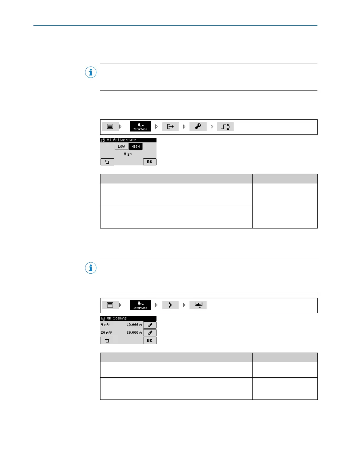
8.3.12 Defining the active state for service functions
NOTE
The procedure for configuring switching outputs Q1 through Q4 is identical. The configu‐
ration is illustrated on switching output Q1.
The active state describes the relationship between the switching state (active or inac‐
tive) and the voltage present on the digital output (high or low) (see "Switching func‐
tions", page 16).
Parameter Factory setting
LOW:
Output potential for active switching state: low voltage
Output potential for inactive switching state: high voltage
LOW
HIGH:
Output potential for active switching state: high voltage
Output potential for inactive switching state: low voltage
8.3.13 Configuring the QA analog output
Scaling the analog output signal to the distance values (see "Analog output", page 44).
NOTE
The analog output signal is inverted if the distance value for the lower analog output
limit (4 mA) is defined to be larger than the distance value for the upper analog output
limit (20 mA), that means if the output current is reduced as the distance increases.
Parameter Factory setting
4 mA:
Distance value for lower analog output signal: -4500 m to 4500 m
10 m
20 mA:
Distance value for upper analog output signal:
-4500 m to 4500 m
20 m
REFERENCE 8
8019329/12TZ/2019-03-28 | SICK O P E R A T I N G I N S T R U C T I O N S | DT1000 and DL1000
67
Subject to change without notice
 Loading...