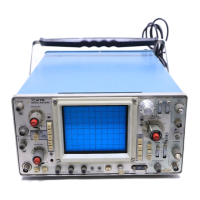
Circuit Description—455/A2/B2
VERTICAL OUTPUT AMPLIFIER ^
The Vertical Output Amplifier circuit provides the final
amplification for the vertical deflection signal. This circuit
includes the Delay Line, the Delay-Line Driver, the Normal
Trigger Pickoff, the Vertical Output Amplifier, and part of
the Beam Finder circuitry. Pushing the BEAM FINDER
pushbutton compresses an overscanned display to within
the viewing area.
Delay-Line Driver
The output from the Channel switching gates, at pin 17 and
18 of U4160, is applied to the Delay-Line-Driver transistors
Q4362 and Q4372. Transistors Q4362 and Q4372 are con
nected as feedback amplifiers with R4362 and R4372
providing the feedback. A sample of the signal at the collec
tor of Q4372 is picked off for the normal trigger signal
supplied to the Horizontal Module.
Resistors R4365 and R4375 provide reverse termination for
the Delay Line. The TRIG VIEW switch S4380 connects
the output of the Trigger view circuit, in the Horizontal
Module, to the input of the Delay Line in place of the signal
from the Delay-Line Driver. This allows viewing of the
trigger signal that is present in the A Trigger circuit in the
Horizontal Module.
Delay-line impedance is 75 £2 and provides a 120 ns delay.
Normal Trigger Pickoff
Normal trigger signals are picked off from the collector of
Q4372 and sent through emitter-follower transistor Q4394
and on to the Horizontal Module.
Resistors R4386, and 75 £2 line termination (Horizontal
Module) divide the signal at the emitter of Q4384 to the
appropriate signal level for the trigger.
Vertical Output Amplifier
Transistors Q4434, Q4444, Q4462, Q4464, Q4466, Q4472,
Q4474 and Q4476 compose a common-emitter shunt-feed
back amplifier. Shunt-feedback transistors Q4462, Q4464,
Q4466 and Q4472, Q4474, Q4476 are stacked to eliminate
the need for a heat sink and a high-voltage transistor. Feed
back is provided through R4473, R4474, R4475 and R4463,
R4464, R4465. Feedback compensation capacitors C4464
and C4474 are an integral part of the circuit board.
The sensitivity at the delay-line input to each amplifier half
is 50 mV/division and at the input to the crt is about 1.35
volts/division. Thus, the gain of the Vertical Output Ampli
fier is about 27. The gain is adjustable with calibration
adjustment R4436.
Thermal resistor RT4437 provides gain temperature com
pensation. Variable-capacitance diode CR4437 and capa
citor C4437 are used for temperature compensation of the
step response; thermal resistor RT4448 varies the bias on
CR4437 as the temperature changes. Capacitor C4417 and
R4417 provide crt rolloff compensation. Capacitor-resistor
combinations C4411, R4411,C4410, C4412, R4412, and
C4414, R4414 are provided for Delay-Line compensation.
When the BEAM FINDER pushbutton in the Main Module
is pressed, +5 volts is applied to the common-emitter stage
through R4435 and R4445. This limits the vertical
deflection to within the crt-screen area.
REV. A, OCT 1975
4-11

 Loading...