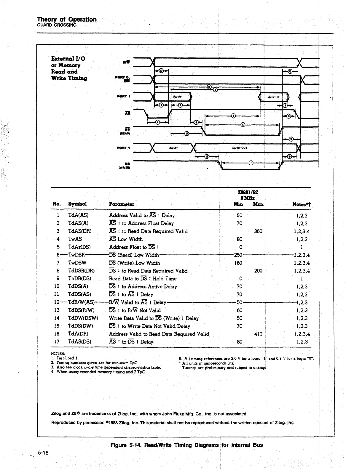
Theory
of
Operation
GUARD
CROSSING
External
VO
or
Memory
Read
and
Write
Timing
Z8601/82
8Mgr
No.
Sprnbol
PmcamoW
Min
Max
NO#
1
TdA(AS) Address Valid to
t
Delay
50 1.2,3
2
TdAS(A)
AS
t
to Address Fjoat Delay
70
1.2.3
3
TdAS(DR)
AS
t
to Read Data Required Valid
360 1.2,3.4
4 TwAS
Low
Width
80
1.2,3
5 TdAdDS) Address Float to
n3
1
0
1
6- TwDSR (Read)
Low
Width
250
1,2.3.4
7 TwDSW
rn
(Write)
Low
Width
160 1 23.4
-
8
TdDSR(DR) DS
1
to Read Data Required Valid
200
1,2.3,4
9
ThDR(DS) Read Data to
t
Hold Time
0
1
-
10 TdDS(A) DS
1
to
Address Actwe
Delay
70 1,2,3
11
TdDS(AS)
m
t
to
a
1
Delay
70 1.2,3
~~-T~WW(AS)----~
Vahd
to
a
f
Delay
50
L2,3
13 TdDS(WW)
t
to Not Valid
60
1,2.3
14 TdDW(DSW) Wrlte Data Valid to (Write)
1
Delay
50 1,2,3
IS
TdDS(DW)
1
to Write Data Not Valid Delay
70
1.2,3
16 TdA(DR) Address Vahd to Read
Data
Requtred Valid
410
1.2,3,4
17 TdAS(DS)
1
to
rn
I
Delay
80
1.2.3
NOTES:
1.
Test
Load
1
5
All trmrnq references
use
2.0
V
for
a
loqrc
"1"
and
0.8
V
for
a
loqrc
"0.
2.
Trrninq numbers qrven
are
for mrnirnum
TpC
All units
m
nanosecqnds
(ns).
3.
Also
see
clock cycle tame dependent characterrstrcs table.
t
Trmrnqs are orel~mr~ary and sublect to
chanqe
4.
When
usrnq extended memory trmrnq
add
2
TpC.
Zilog and
280
are trademarks of Zilog. Inc.. with whom John Fluke Mfg. Go.. Inc. is not assoccated.
Reproduced
by
permission
01983
Zilog.
Inc.
Th~s
material shall not
be
reproduced without the wrctten conseht of Z~log. Inc.
I
Figure
5-14.
Readwrite Timing Diagrams for
Internal
Bus
Artisan Technology Group - Quality Instrumentation ... Guaranteed | (888) 88-SOURCE | www.artisantg.com
 Loading...