5.5 Power Amplifier (PA)
5-34
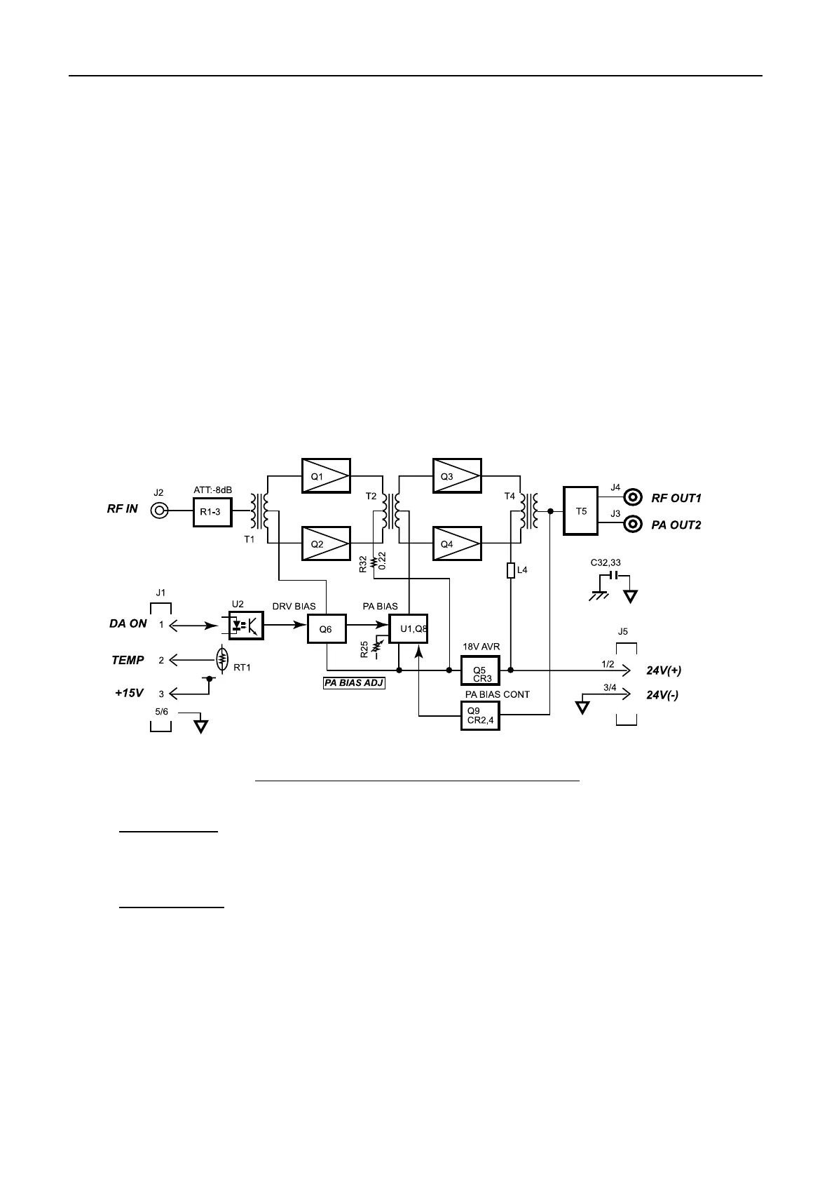
5.5.2 FS-2570T DRV board (05P0738)
The amplifier circuit on DRV board consists of drivers, Q1 and Q2 and PA push-pull
amplifiers, Q3 and Q4 and power distribution circuits, T5. The gain is about 20 dB. 0.3
W (about 10 Vp-p) RF signal from TX/RX board is boosted up and then divided by T5.
The output is about 15 W at “RF OUT-1” and “RF OUT-2”.
PA bias current is adjusted to 100 mA by R25. When measuring the current, the
ammeter is placed in series to L4 in PA Vc circuit.
The output of T4 is connected to PA bias control circuit, Q9, CR2 and CR4. Q9 turns on
with the T/R output power of 60 to 70 W and appropriate PA bias is selected to reduce
intermodulation distortion (IMD). The driver bias is about
30 to 40 mA. To check the
bias current, measure the voltage across R32 (0.22 Ω) and use formula,
I
BIAS
=V
R32
/0.22.
The ground of PA board is isolated by C32 and C33 from chassis ground. When
measuring voltage, use the ground on DRV board.
Fig.5.5.3 Block diagram of FS-2570 DRV board
TEMP Signal
The thermistor RT1 detects the PA temperature. Data is not used.
DA ON Signal
DA ON signal switches on/off the bias circuit on DRV board.
 Loading...