5.5 Power Amplifier (PA)
5-35
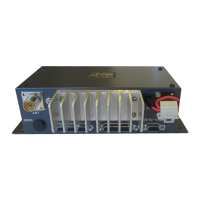
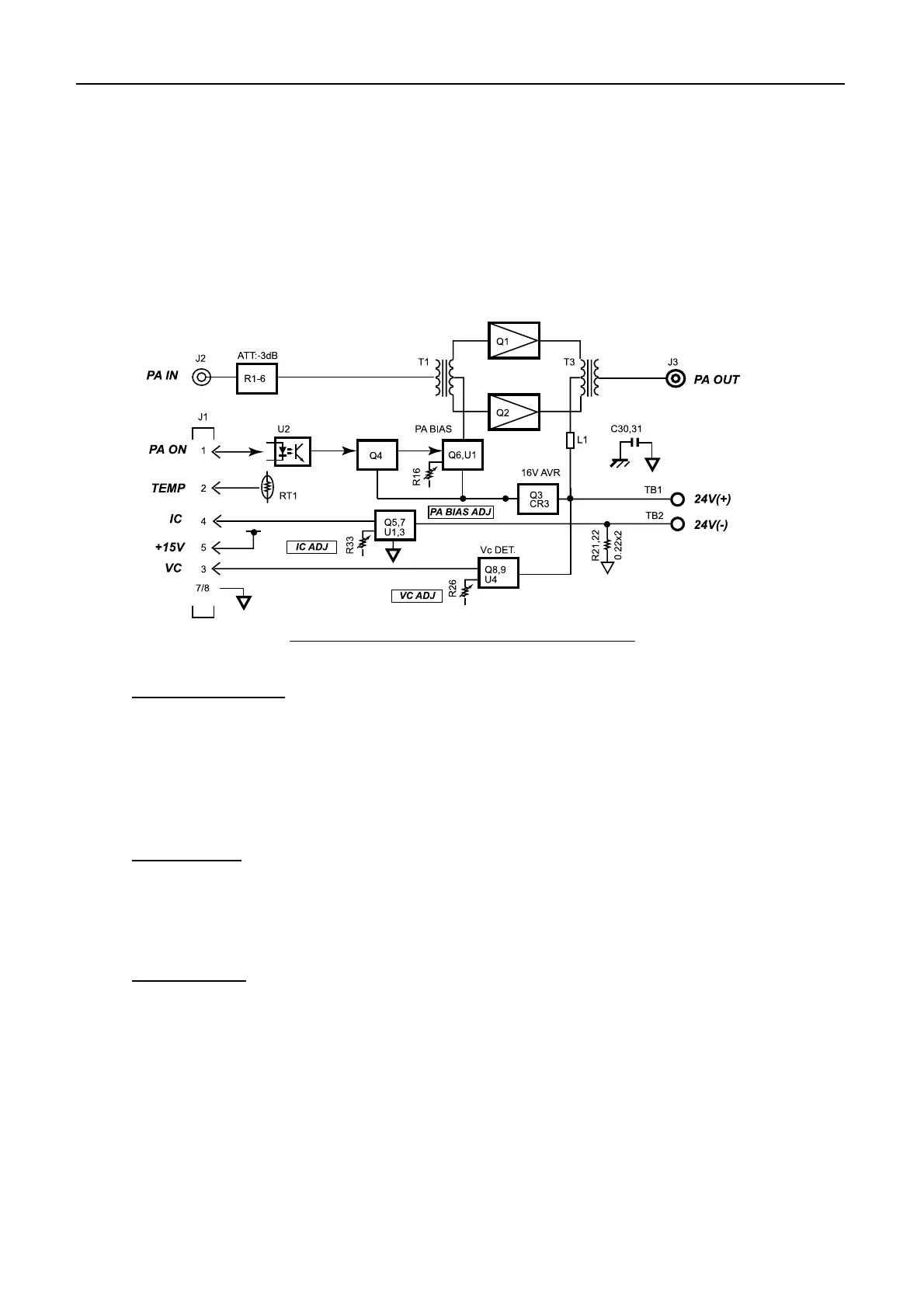
5.5.3 FS-2570T PA board (05P0739)
The amplifier circuit on PA board consists of push-pull circuits, Q1 and Q2. The gain is
about 10 dB. 15 W RF signal from DRV board is boosted up about 150 W.
PA bias current is adjusted to 200 mA by R16. When measuring the current, the
ammeter is placed in series to L1 in PA Vc circuit.
The ground of PA board is isolated by C30 and C31 from chassis ground. When
measuring voltage, use the ground on PA board.
Fig.5.5.4 Block diagram of FS-2570 PA board
VC and IC Signals
PA collector voltage (VC) is adjusted by R26. The VC detector consisting of U4, Q8
and Q9 sends VC to TX FIL board. VC is displayed numerically in Power SET UP
menu. The displayed VC is the one detected on PA-1 board. PA collector current (IC) is
adjusted by R33. The current is detected by R21 and R22 and displayed in Power
SETUP menu as “IC”. The displayed IC is the sum of Ics on PA-1 and PA-2 board.
TEMP Signal
The thermistor RT1 detects the temperature of power amplifier. When the temperature
increases up to about 80 °C, “TX POW REDUCED MAIN AMP HEATED” appears
and the power is reduced automatically.
PA ON Signal
PA ON signal switches on/off the bias circuit on PA board.
 Loading...