RL78/G13 CHAPTER 12 SERIAL ARRAY UNIT
R01UH0146EJ0100 Rev.1.00 680
Sep 22, 2011
12.8.1 Address field transmission
Address field transmission is a transmission operation that first executes in I
2
C communication to identify the target for
transfer (slave). After a start condition is generated, an address (7 bits) and a transfer direction (1 bit) are transmitted in
one frame.
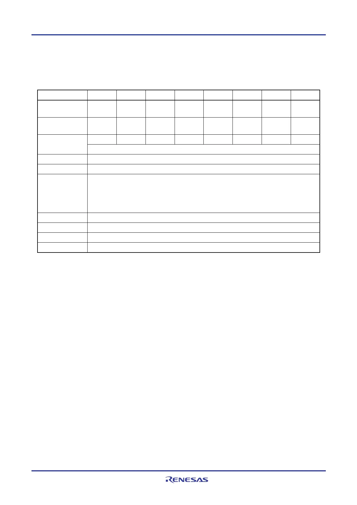
Simplified I
2
C
IIC00 IIC01 IIC10 IIC11 IIC20 IIC21 IIC30 IIC31
Target channel Channel 0
of SAU0
Channel 1
of SAU0
Channel 2
of SAU0
Channel 3
of SAU0
Channel 0
of SAU1
Channel 1
of SAU1
Channel 2
of SAU1
Channel 3
of SAU1
Pins used SCL00,
SDA00
Note
SCL01,
SDA01
Note
SCL10,
SDA10
Note
SCL11,
SDA11
Note
SCL20,
SDA20
Note
SCL21,
SDA21
Note
SCL30,
SDA30
Note
SCL31,
SDA31
Note
INTIIC00 INTIIC01 INTIIC10 INTIIC11 INTIIC20 INTIIC21 INTIIC30 INTIIC31 Interrupt
Transfer end interrupt only (Setting the buffer empty interrupt is prohibited.)
Error detection flag Parity error detection flag (PEFmn)
Transfer data length 8 bits (transmitted with specifying the higher 7 bits as address and the least significant bit as R/W control)
Transfer rate Max. fMCK/2 [Hz] (SDRmn[15:9] = 1 or more) fMCK: Operation clock frequency of target channel
However, the following condition must be satisfied in each mode of I
2
C.
• Max. 1 MHz (first mode plus)
• Max. 400 kHz (first mode)
• Max. 100 kHz (standard mode)
Data level Forward output (default: high level)
Parity bit No parity bit
Stop bit Appending 1 bit (for ACK reception timing)
Data direction MSB first
Note To perform communication via simplified I
2
C, set the N-ch open-drain output (VDD tolerance) mode (POM03,
POM11, POM14, POM50, POM53, POM71, POM74, POM143 = 1) for the port output mode registers (POM0,
POM1, POM4, POM5, POM7 to POM9, POM14) (see 4.3 Registers Controlling Port Function for details). When
IIC00, IIC10, IIC20, IIC30, IIC31 communicating with an external device with a different potential, set the N-ch
open-drain output (V
DD tolerance) mode (POM04, POM10, POM15, POM54, POM142 = 1) also for the clock
input/output pins (SCL00, SCL10, SCL20, SCL30, SCL31) (see 4.4.4 Connecting to external device with
different potential (2.5 V, 3 V) for details).
Remark m: Unit number (m = 0, 1), n: Channel number (n = 0 to 3), mn = 00 to 03, 10 to 13
<R>

 Loading...


