RL78/G13 CHAPTER 26 ON-CHIP DEBUG FUNCTION
R01UH0146EJ0100 Rev.1.00 953
Sep 22, 2011
26.2 On-Chip Debug Security ID
The RL78/G13 has an on-chip debug operation control bit in the flash memory at 000C3H (see CHAPTER 24 OPTION
BYTE) and an on-chip debug security ID setting area at 000C4H to 000CDH, to prevent third parties from reading memory
content.
When the boot swap function is used, also set a value that is the same as that of 010C3H and 010C4H to 010CDH in
advance, because 000C3H, 000C4H to 000CDH and 010C3H, and 010C4H to 010CDH are switched.
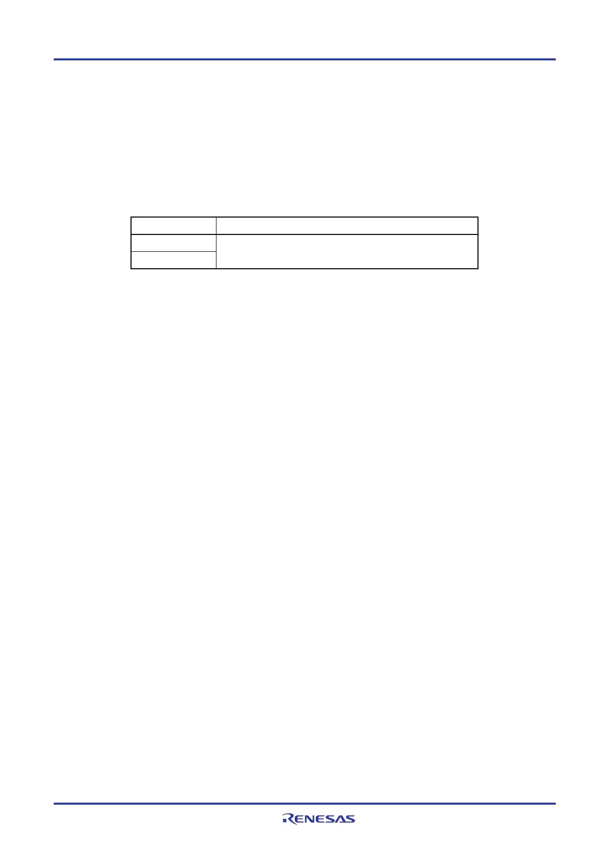
Table 26-1. On-Chip Debug Security ID
Address On-Chip Debug Security ID
000C4H to 000CDH
010C4H to 010CDH
Any ID code of 10 bytes
26.3 Securing of User Resources
To perform communication between the RL78/G13 and E1 on-chip debugging emulator, as well as each debug function,
the securing of memory space must be done beforehand.
If Renesas Electronics assembler or compiler is used, the items can be set by using linker options.
(1) Securement of memory space
The shaded portions in Figure 26-2 are the areas reserved for placing the debug monitor program, so user
programs or data cannot be allocated in these spaces. When using the on-chip debug function, these spaces must
be secured so as not to be used by the user program. Moreover, this area must not be rewritten by the user
program.

 Loading...


