RL78/G13 CHAPTER 25 FLASH MEMORY
R01UH0146EJ0100 Rev.1.00 932
Sep 22, 2011
25.1.1 Programming Environment
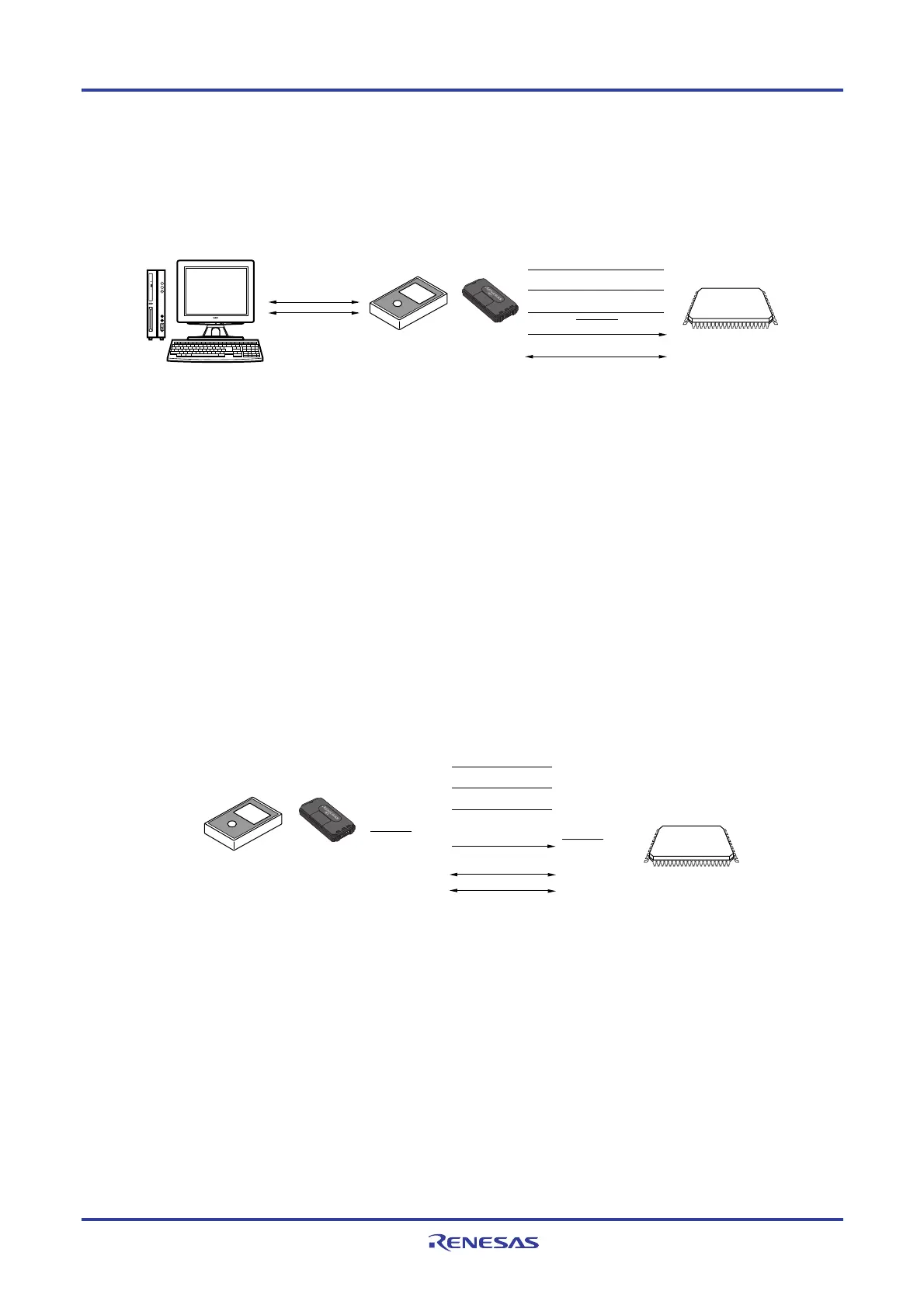
The environment required for writing a program to the flash memory of the RL78/G13 is illustrated below.
Figure 25-1. Environment for Writing Program to Flash Memory
RS-232C
USB
RL78/G13
EV
DD
Note
V
DD
V
SS
, EV
SS
RESET
TOOL0 (dedicated single-line UART)
Host machine
Dedicated flash
memory programmer
PG-FP5, FL-PR5
E1
Note 64-pin, 80-pin, 100-pin and 128-pin products only.
A host machine that controls the dedicated flash memory programmer is necessary.
To interface between the dedicated flash memory programmer and the RL78/G13, the TOOL0 pin is used for
manipulation such as writing and erasing via a dedicated single-line UART. To write the flash memory off-board, a
dedicated program adapter (FA series) is necessary.
25.1.2 Communication Mode
Communication between the dedicated flash memory programmer and the RL78/G13 is established by serial
communication using the TOOL0 pin via a dedicated single-line UART of the RL78/G13.
Transfer rate: 1 M, 500 k, 250 k, 115.2 kbps
Figure 25-2. Communication with Dedicated Flash Memory Programmer
VDD/EVDD
VSS/EVSS/REGC
Note 3
RESET
TOOL0
EV
DD
VDDVDD
GND
RESET
Note 1
,
/RESET
Note 2
RL78/G13
Dedicated flash
memory programmer
PG-FP5, FL-PR5
E1
TOOL0
Note 1
SI/RxD
Note 2
Notes 1. When using E1 on-chip debugging emulator.
2. When using PG-FP5 or FL-PR5.
3. Connect REGC pin to ground via a capacitor (default: 0.47
μ
F).
<R>

 Loading...


