3
© 2009 - 2011 TOSHIBA TEC CORPORATION All rights reserved e-STUDIO555/655/755/855
COPY PROCESS
3 - 1
3. COPY PROCESS
3.1 General Description
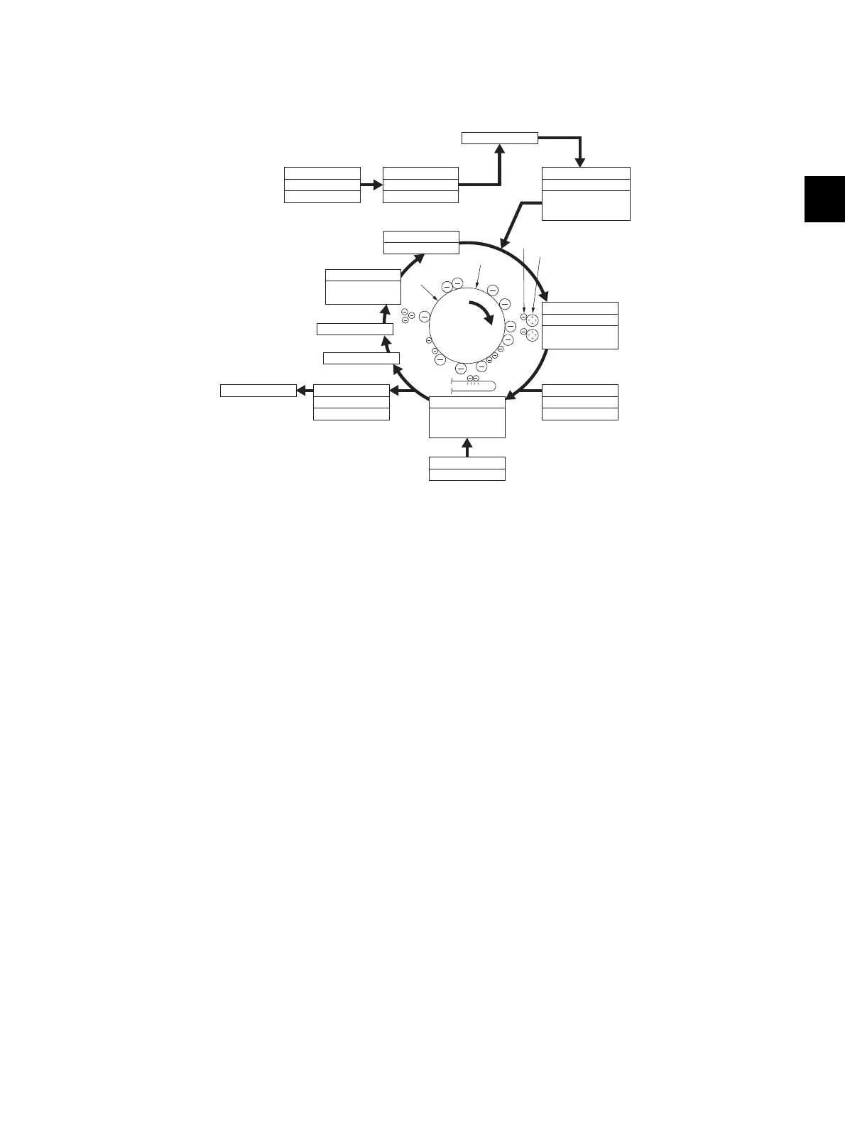
Fig. 3-1
(1) Charging:
Negatively charges the surface of the
photoconductive drum.
↓
(6) Transfer:
Transfers the visible image on the
photoconductive drum onto paper.
Separation:
Separates the paper from the drum
together with the toner.
↓
(2) Original exposure:
Converts images on the original into optical
signals.
↓
(7) Fusing:
Fuses the toner onto the paper by applying
heat and pressure.
↓
(3) Scanning:
Converts image optical signals into
electrical signals.
↓
(8) Brush cleaning:
Cleans dirt and paper dust on the drum.
↓
(4) Writing:
Converts image electrical signals into
optical signals (laser emission) and
exposes them to the surface of the
photoconductive drum.
↓
(9) Blade cleaning:
Forcibly removes the residual toner on the
drum.
↓
(5) Development:
Makes the negatively-charged toner
adhere to the photoconductive drum and
forms a visible image.
↓
(10)Discharging:
Discharges any remaining negative charge
on the drum.
Scanning
CCD
600 dpi,7500 pixel
(
3
)
Original exposure
Xenon lamp
29W
(
2
)
Image processing
Bypass feeding
Discharge
LED array
(
Wavelength 660nm x14pcs
)
-500V
(
-300V~-900V
)
(
10
)
Drawer feeding
LCF feeding
FusingDischarging
Fuser roller
700~1450W
(
4
)
Writing
Semiconductive laser
Pw=3.9 nJ/mm
2
(
555/655
)
Pw=3.0 nJ/mm
2
(755/855)
(
9
)
(
1
)
Charging
(
grid voltage
)
Bias
-394V
(
-200~-800
)
DC+AC
5 µA
(
5
)
(
6
)
(
7
)
Development
Magnetic roller
Transfer/Separation
Cleaning brush + Blade
Blade cleaning
(
8
)
Brush cleaning
Toner
Carrier
70 µA
(555/655/755)
85 µA
(855)
 Loading...