VCU118 Board User Guide 21
UG1224 (v1.0) December 15, 2016
www.xilinx.com
Chapter 3: Board Component Descriptions
I/O Voltage Rails
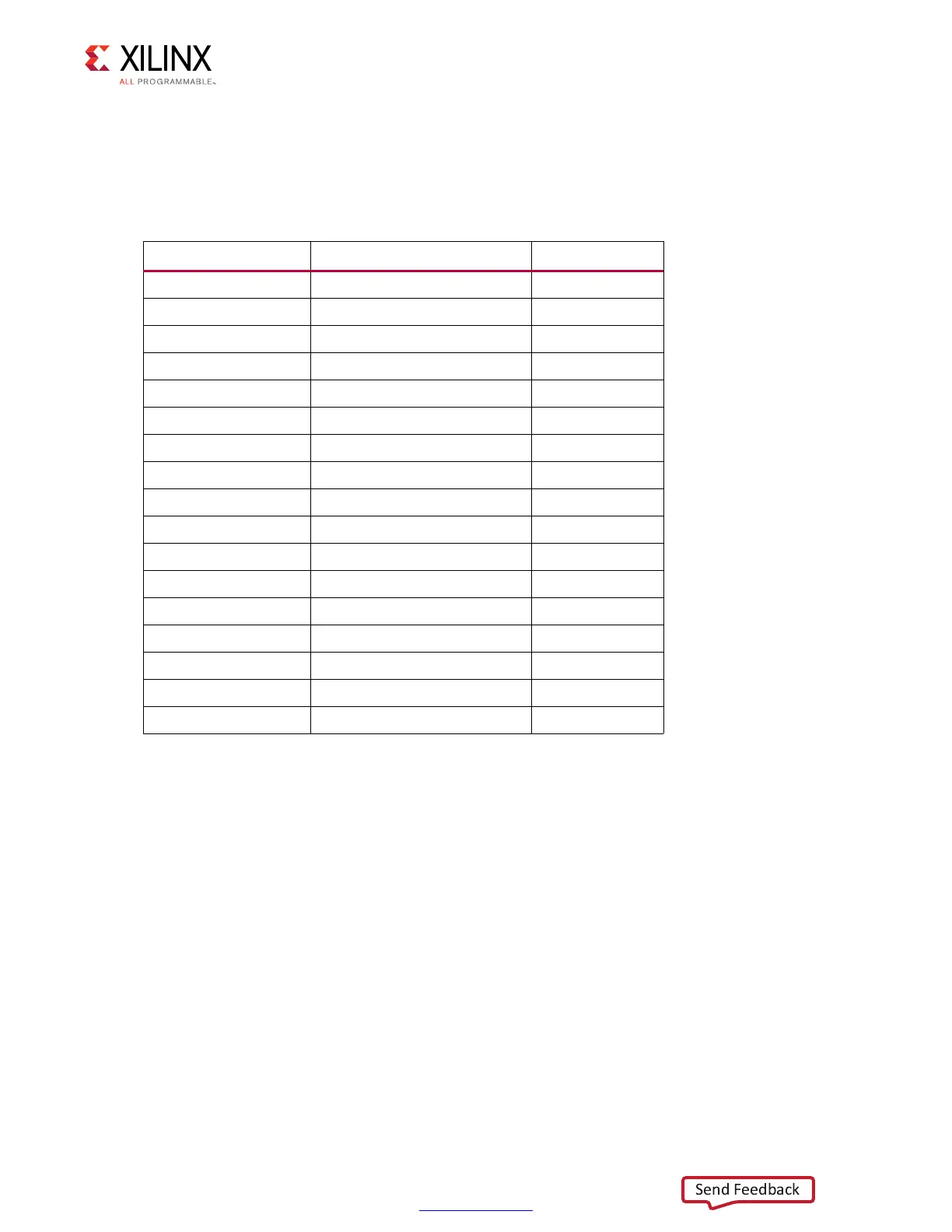
There are 16 I/O banks available on the XCVU9P device and the VCU118 board. The voltages
applied to the FPGA I/O banks used by the VCU118 board are listed in Table 3-1.
Table 3-1: I/O Bank Voltage Rails
FPGA (U1) Bank Power Supply Rail Net Name Voltage
Bank 0 VCC1V8_FPGA 1.8V
HP Bank 40 VCC1V2_FPGA 1.2V
HP Bank 41 VCC1V2_FPGA 1.2V
HP Bank 42 VCC1V2_FPGA 1.2V
HP Bank 43 VADJ_1V8_FPGA 1.8V
HP Bank 45 VADJ_1V8_FPGA 1.8V
HP Bank 46 VCC1V2_FPGA 1.2V
HP Bank 47 VCC1V2_FPGA 1.2V
HP Bank 48 VCC1V2_FPGA 1.2V
HP Bank 64 VCC1V8_FPGA 1.8V
HP Bank 65 VCC1V8_FPGA 1.8V
HP Bank 66 VADJ_1V8_FPGA 1.8V
HP Bank 67 VADJ_1V8_FPGA 1.8V
HP Bank 70 VADJ_1V8_FPGA 1.8V
HP Bank 71 VCC1V2_FPGA 1.2V
HP Bank 72 VCC1V2_FPGA 1.2V
HR Bank 73 VCC1V2_FPGA 1.2V

 Loading...


