VCU118 Board User Guide 44
UG1224 (v1.0) December 15, 2016
www.xilinx.com
Chapter 3: Board Component Descriptions
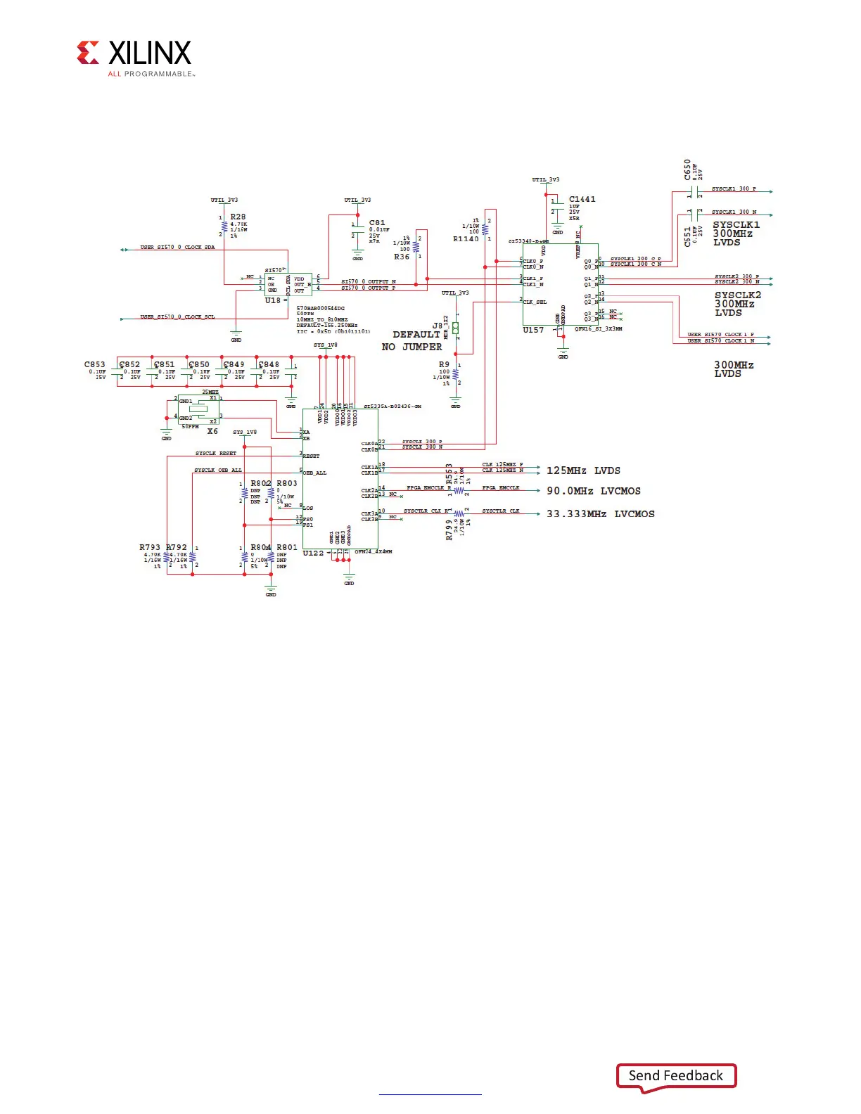
The 300 MHz system clock circuit (U122 upper right CLK0 branch) is shown in Figure 3-4.
The VCU118 SYSCLKn_300 clocks have an optional clock oscillator source U18 as shown in
Figure 3-4. SI570 I
²
C programmable low-jitter 3.3V LVDS differential oscillator U18 is
connected to the CLK1 P/N inputs (pins 3 (P) and 4 (N)) of clock MUX/quad buffer SI53340
U157.
The clock MUX input select pin 2 is wired to 2-pin header J8 and a pull-down resistor. The
default J8 setting is jumper OFF, which allows the pull-down resistor to select U157 input
CLK0, the SI5335A quad clock generator U122 CLK0 300 MHz fixed frequency output. SI570
U18 is selected as the U157 source clock when a jumper block is installed on J8, pulling the
U157 select signal High and selecting the U157 CLK1 input. SI570 U18 can be programmed
over the IIC_MAIN bus, either from the FPGA U1 fabric or the Zynq-7000 AP SoC system
controller U111. See the I2C Bus, Topology, and Switches section for more details.
X-Ref Target - Figure 3-4
Figure 3-4: VCU118 System Clock

 Loading...


