VCU118 Board User Guide 61
UG1224 (v1.0) December 15, 2016
www.xilinx.com
Chapter 3: Board Component Descriptions
Quad 233:
• MGTREFCLK0 - MGT_SI570_CLOCK3_C_P/N (U104)
• MGTREFCLK1 - MGT233_CLK1_P/N (SMA J33 P, J32 N)
• Four GTY transceivers allocated to FIREFLY (J6)
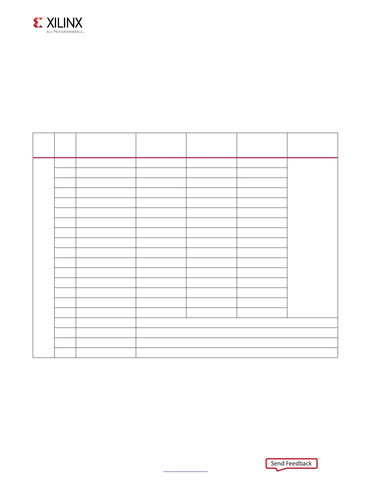
Table 3-14 through Table 3-20 list the VCU118 FPGA U1 GTY transceiver bank 224, 225, 226,
227, 231, 232 and 233 connections, respectively.
Table 3-14: VCU118 FPGA U1 GTY Transceiver Bank 224 Connections
MGT
Bank
FPGA
(U1)
Pin
FPGA (U1) Pin
Name
Schematic Net
Name
Connected Pin
Connected Pin
Name
Connected
Device
GTY
Bank
224
BE5 MGTYTXP0_224 PCIE_TX15_P A80 HSIP(15)
PCIe EDGE Conn.
U2
BE4 MGTYTXN0_224 PCIE_TX15_N A81 HSIN(15)
BB2 MGTYRXP0_224 PCIE_RX15_P B78 HSOP(15)
BB1 MGTYRXN0_224 PCIE_RX15_N B79 HSON(15)
BC5 MGTYTXP1_224 PCIE_TX14_P A76 HSIP(14)
BC4 MGTYTXN1_224 PCIE_TX14_N A77 HSIN(14)
AY2 MGTYRXP1_224 PCIE_RX14_P B74 HSOP(14)
AY1 MGTYRXN1_224 PCIE_RX14_N B75 HSON(14)
BA5 MGTYTXP2_224 PCIE_TX13_P A72 HSIP(13)
BA4 MGTYTXN2_224 PCIE_TX13_N A73 HSIN(13)
AV2 MGTYRXP2_224 PCIE_RX13_P B70 HSOP(13)
AV1 MGTYRXN2_224 PCIE_RX13_N B71 HSON(13)
AW5 MGTYTXP3_224 PCIE_TX12_P A68 HSIP(12)
AW4 MGTYTXN3_224 PCIE_TX12_N A69 HSIN(12)
AT2 MGTYRXP3_224 PCIE_RX12_P B66 HSOP(12)
AT1 MGTYRXN3_224 PCIE_RX12_N B67 HSON(12)
AR9 MGTREFCLK0P_224 NC
AR8 MGTREFCLK0N_224 NC
AN9 MGTREFCLK1P_224 NC
AN8 MGTREFCLK1N_224 NC

 Loading...


