VCU118 Board User Guide 31
UG1224 (v1.0) December 15, 2016
www.xilinx.com
Chapter 3: Board Component Descriptions
RLD3 Component Memory
[Figure 2-1, callout 5]
The 288 MB RLD3 72-bit wide component memory system is comprised of two 36-bit 1.125
Gb RLDRAM3 devices (Micron MT44K32M36RB-083E) located at U141-U142. This memory
system is connected to the XCVU9P HP banks 46, 47, and 48. The RLD3 0.6V VTT termination
voltage (net RLD3_C3_VTT) is sourced from TI TPS51200DR linear regulator U143. The RLD3
memory interface bank VREF pins are not connected, which, coupled with an XDC
set_property INTERNAL_VREF constraint, invoke the INTERNAL VREF mode. The
connections between the RLD3 component memories and XCVU9P banks 46, 47, and 48 are
listed in Table 3-4.
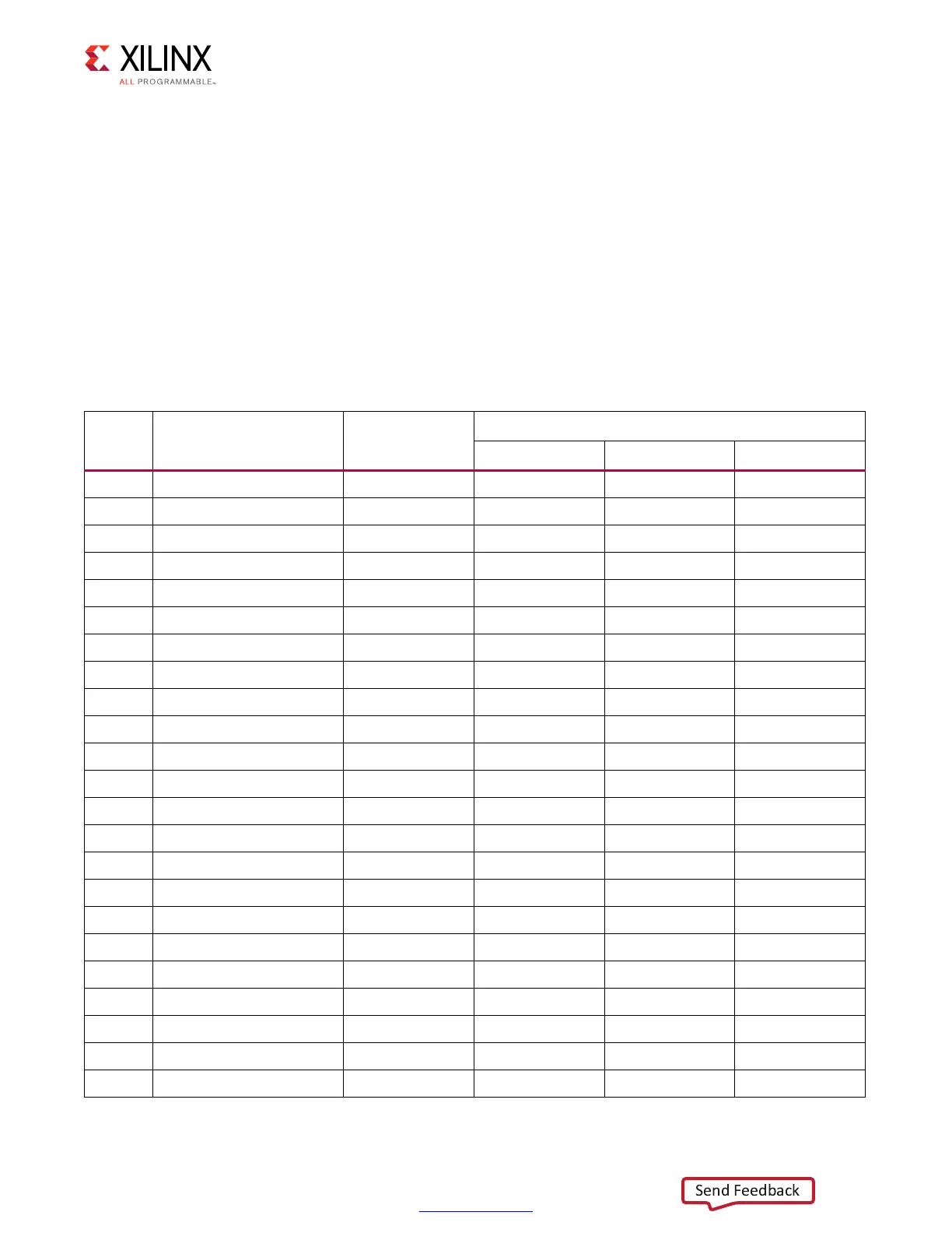
Table 3-4: RLD3 Memory 72-bit I/F to FPGA U1 Banks 46, 47, and 48
FPGA
(U1) Pin
Schematic Net Name I/O Standard
Component Memory
Pin # Pin Name Ref. Des.
H39 RLD3_C3_72B_DQ0 SSTL12 D11 DQ0 U141
H40 RLD3_C3_72B_DQ1 SSTL12 E10 DQ1 U141
G40 RLD3_C3_72B_DQ2 SSTL12 C8 DQ2 U141
F40 RLD3_C3_72B_DQ3 SSTL12 C10 DQ3 U141
H38 RLD3_C3_72B_DQ4 SSTL12 C12 DQ4 U141
G38 RLD3_C3_72B_DQ5 SSTL12 B9 DQ5 U141
K37 RLD3_C3_72B_DQ6 SSTL12 B11 DQ6 U141
J37 RLD3_C3_72B_DQ7 SSTL12 A8 DQ7 U141
F38 RLD3_C3_72B_DQ8 SSTL12 A10 DQ8 U141
J35 RLD3_C3_72B_DQ9 SSTL12 J10 DQ9 U141
H35 RLD3_C3_72B_DQ10 SSTL12 K11 DQ10 U141
J36 RLD3_C3_72B_DQ11 SSTL12 K13 DQ11 U141
H37 RLD3_C3_72B_DQ12 SSTL12 L8 DQ12 U141
H34 RLD3_C3_72B_DQ13 SSTL12 L10 DQ13 U141
G35 RLD3_C3_72B_DQ14 SSTL12 L12 DQ14 U141
F35 RLD3_C3_72B_DQ15 SSTL12 M9 DQ15 U141
F36 RLD3_C3_72B_DQ16 SSTL12 M11 DQ16 U141
G36 RLD3_C3_72B_DQ17 SSTL12 N8 DQ17 U141
E37 RLD3_C3_72B_DQ18 SSTL12 D3 DQ18 U141
E38 RLD3_C3_72B_DQ19 SSTL12 E4 DQ19 U141
C39 RLD3_C3_72B_DQ20 SSTL12 C6 DQ20 U141
B40 RLD3_C3_72B_DQ21 SSTL12 C4 DQ21 U141
A39 RLD3_C3_72B_DQ22 SSTL12 C2 DQ22 U141

 Loading...


