VCU118 Board User Guide 48
UG1224 (v1.0) December 15, 2016
www.xilinx.com
Chapter 3: Board Component Descriptions
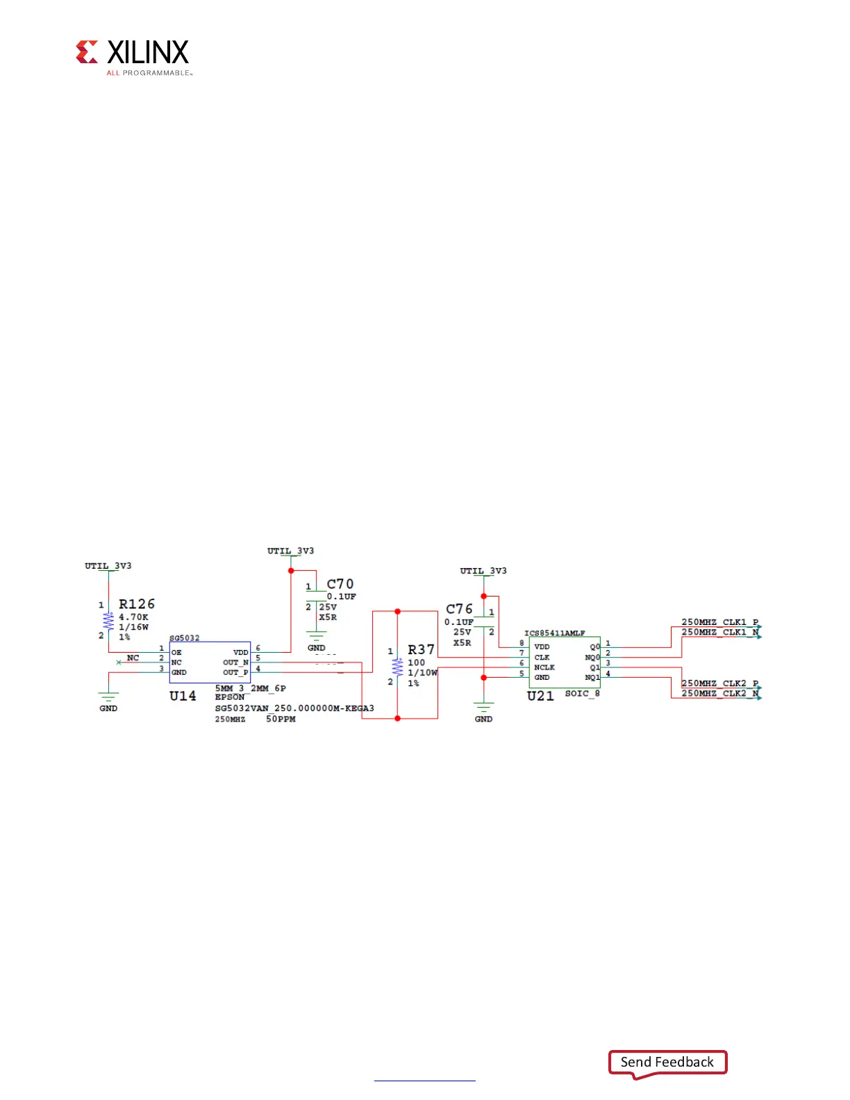
250 MHz Clock
[Figure 2-1, callout 14]
The VCU118 evaluation board has an Epson SG5032 3.3V LVDS differential fixed 250 MHz
oscillator (U14) connected to 1-to-2 ICS85411 clock buffer U21.
The 3.3V ICS85411 U21 has two LVDS output clock pairs:
• U21 output Q0 drives clock pair 250MHZ_CLK1_P/N, connected to XCVU9P FPGA U1 HP
bank 71 GC pins E12 and D12, respectively.
• U21 output Q1 drives clock pair 250MHZ_CLK2_P/N, connected to XCVU9P FPGA U1 HP
bank 41 GC pins AW26 and AW27, respectively.
The ICS85411 U21 oscillator is a fixed frequency device:
• Epson SG5032VAN_250.000000M-KEGA3
• Frequency tolerance: 50 ppm
• 3.3V LVDS differential output
The SG5032 U14/ICS85411A U14/U21 clock circuit is shown in Figure 3-7.
X-Ref Target - Figure 3-7
Figure 3-7: VCU118 Board 250 MHz Clocks
250MHZ_N
250MHZ_P
X18001-112216

 Loading...


