VCU118 Board User Guide 62
UG1224 (v1.0) December 15, 2016
www.xilinx.com
Chapter 3: Board Component Descriptions
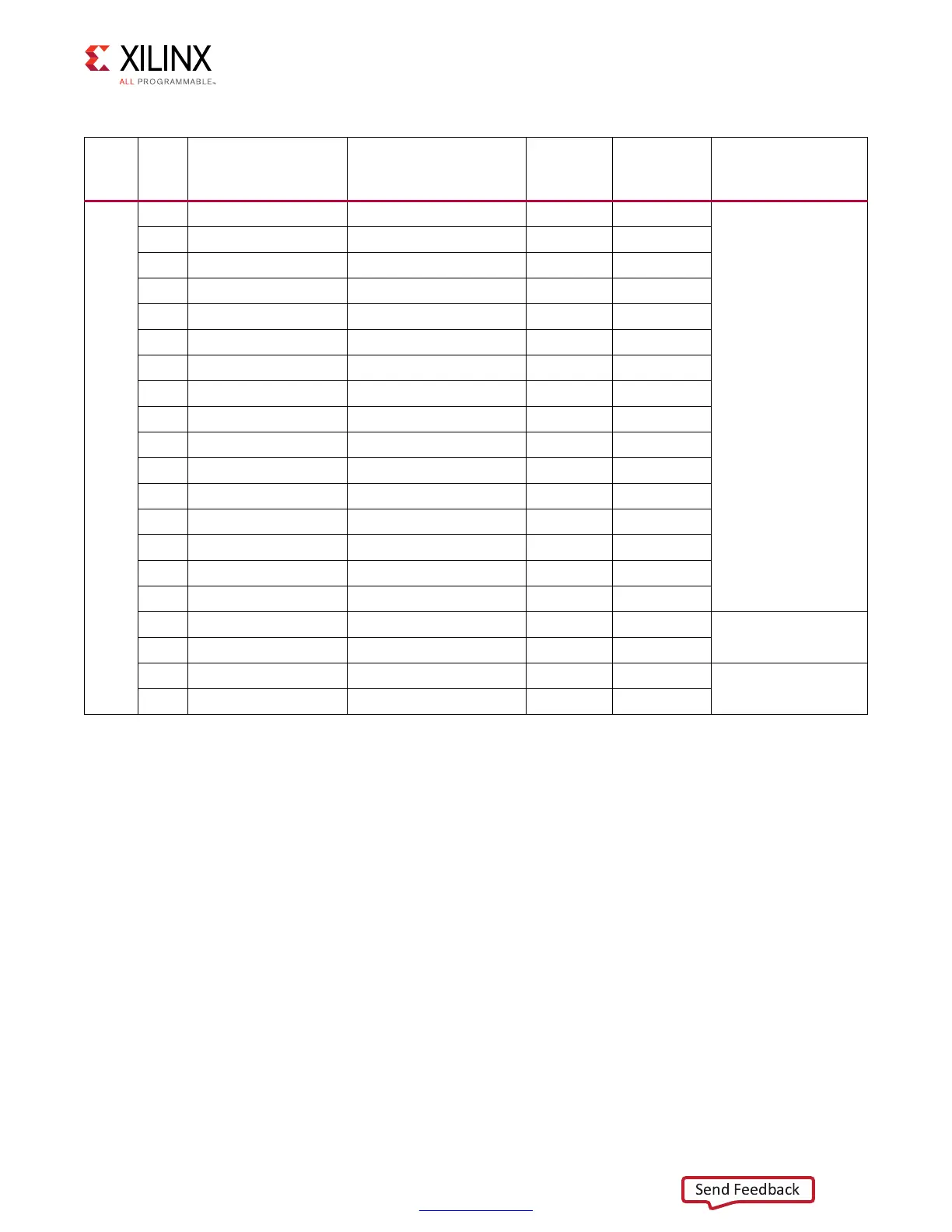
Table 3-15: VCU118 FPGA U1 GTY Transceiver Bank 225 Connections
MGT
Bank
FPGA
(U1)
Pin
FPGA (U1) Pin Name Schematic Net Name
Connected
Pin
Connected
Pin Name
Connected Device
GTY
Bank
225
AU5 MGTYTXP0_225 PCIE_TX11_P A64 HSIP(11)
PCIe EDGE Conn. U2
AU4 MGTYTXN0_225 PCIE_TX11_N A65 HSIN(11)
AP2 MGTYRXP0_225 PCIE_RX11_P B62 HSOP(11)
AP1 MGTYRXN0_225 PCIE_RX11_N B63 HSON(11)
AT7 MGTYTXP1_225 PCIE_TX10_P A60 HSIP(10)
AT6 MGTYTXN1_225 PCIE_TX10_N A61 HSIN(10)
AM2 MGTYRXP1_225 PCIE_RX10_P B58 HSOP(10)
AM1 MGTYRXN1_225 PCIE_RX10_N B59 HSON(10)
AR5 MGTYTXP2_225 PCIE_TX9_P A56 HSIP(9)
AR4 MGTYTXN2_225 PCIE_TX9_N A57 HSIN(9)
AK2 MGTYRXP2_225 PCIE_RX9_P B54 HSOP(9)
AK1 MGTYRXN2_225 PCIE_RX9_N B55 HSON(9)
AP7 MGTYTXP3_225 PCIE_TX8_P A52 HSIP(8)
AP6 MGTYTXN3_225 PCIE_TX8_N A53 HSIN(8)
AJ4 MGTYRXP3_225 PCIE_RX8_P B50 HSOP(8)
AJ3 MGTYRXN3_225 PCIE_RX8_N B51 HSON(8)
AL9 MGTREFCLK0P_225 PCIE_CLK1_P 1 Q0
U20 ICS85411A clock
buffer
AL8 MGTREFCLK0N_225 PCIE_CLK1_N 2 NQ0
AJ9 MGTREFCLK1P_225 MGT_SI570_CLOCK1_C_P 11 Q1_P
U104 SI53340 clock
buffer
AJ8 MGTREFCLK1N_225 MGT_SI570_CLOCK1_C_N 12 Q1_N

 Loading...


