VCU118 Board User Guide 69
UG1224 (v1.0) December 15, 2016
www.xilinx.com
Chapter 3: Board Component Descriptions
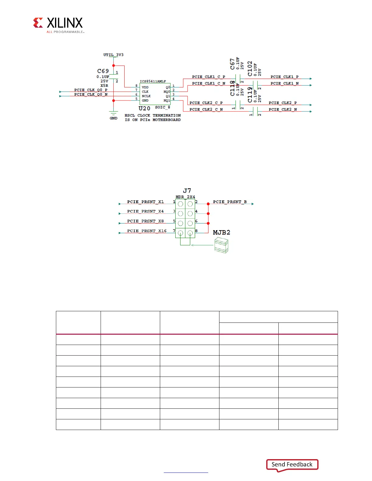
PCIe lane width/size is selected by jumper J7 shown in Figure 3-12. The default lane size
selection is 16-lane (J7 pins 7 and 8 jumpered).
Table 3-21 lists the PCIe U2 edge connector wiring to FPGA U1.
X-Ref Target - Figure 3-11
Figure 3-11: PCIe Clock
X-Ref Target - Figure 3-12
Figure 3-12: PCI Express Lane Size Select Jumper J7
Table 3-21: VCU118 Board FPGA U1 to PCIe Edge U2 Connections
FPGA (U1) Pin
FPGA (U1) Pin
Name
Schematic Net
Name
PCIe Edge U2
Pin Num Pin Name
Y7 MGTYTXP3_227 PCIE_TX0_P A16 HSIN(0)
Y6 MGTYTXN3_227 PCIE_TX0_N A17 HSIP(0)
AB7 MGTYTXP2_227 PCIE_TX1_P A21 HSIN(1)
AB6 MGTYTXN2_227 PCIE_TX1_N A22 HSIP(1)
AD7 MGTYTXP1_227 PCIE_TX2_P A25 HSIN(2)
AD6 MGTYTXN1_227 PCIE_TX2_N A26 HSIP(2)
AF7 MGTYTXP0_227 PCIE_TX3_P A29 HSIN(3)
AF6 MGTYTXN0_227 PCIE_TX3_N A30 HSIP(3)
AH7 MGTYTXP3_226 PCIE_TX4_P A35 HSIP(4)

 Loading...


