VCU118 Board User Guide 43
UG1224 (v1.0) December 15, 2016
www.xilinx.com
Chapter 3: Board Component Descriptions
System Clock
[Figure 2-1, callout 11]
The system clock source is a Silicon Labs SI5335A quad clock generator U122. The system
clock (SYSCLK) is a LVDS 300 MHz clock sourced from the CLK0A output pair of U122.
SYSCLK is wired to SI53340 U157 clock MUX/quad-buffer input CLK0 P/N inputs (pins 6 (P)
and 7 (N)).
The 3.3V SI53340 U157 has four LVDS output clock pairs:
• U157 output Q0 drives clock pair SYSCLK1_300_P/N, connected to XCVU9P FPGA U1
bank 47 global clock (GC) pins G31 and F31 (series capacitor coupled), respectively.
• U157 output Q1 drives clock pair SYSCLK2_300_P/N which is not connected to XCVU9P
FPGA U1, it is wired to the SI53340 U104 CLK1 input.
• U157 output Q2 drives clock pair USER_SI570_CLOCK1_P/N, connected to XCVU9P
FPGA U1 bank 64 global clock (GC) pins AW23 and AW22, respectively.
• U157 output Q3 is not connected.
Clock generator: U122 Silicon Labs SI5335A-B03426-GM (CLK0A 300 MHz)
• Low phase jitter of 0.7 pS RMS
• LVDS differential output
• Quad clock buffer: Silicon Labs SI53340-B-GM (SYSCLK1, SYSCLK2 300 MHz)
• Additive phase jitter of 43 fs RMS
• LVDS differential output
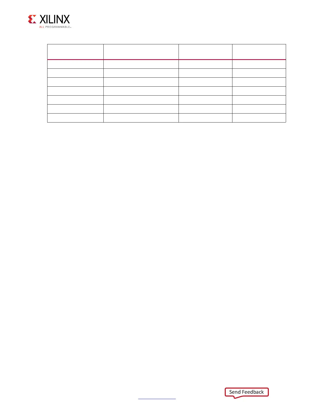
SMA/J35.1 USER_SMA_CLOCK_N LVDS P32
SMA/U38.4 QSFP_SI570_CLOCK_P NA
(2)
W9
SMA/U38.5 QSFP_SI570_CLOCK_N NA
(2)
W8
ICS85411A/U21.1 250MHZ_CLK1_P LVDS E12
ICS85411A/U21.2 250MHZ_CLK1_N LVDS D12
ICS85411A/U21.3 250MHZ_CLK2_P LVDS AW26
ICS85411A/U21.4 250MHZ_CLK2_N LVDS AW27
Notes:
1. Series capacitor coupled, MGT connections I/O standard is not applicable.
2. SI570 U32 SI570_OUTPUT_P/N nets are wired to quad clock buffer U104, (1) also applies.
Table 3-7: VCU118 Clock Sources to XCVU9P FPGA U1 Connections (Cont’d)
Clock Source
Device/U#.Pin#
Schematic Net Name I/O Standard FPGA (U1) Pin

 Loading...


