VCU118 Board User Guide 67
UG1224 (v1.0) December 15, 2016
www.xilinx.com
Chapter 3: Board Component Descriptions
For additional information on GTY transceivers, see UltraScale Architecture GTY Transceivers
User Guide (UG578) [Ref 6]. Also see UltraScale FPGAs Transceivers Wizard LogiCORE IP
Product Guide (PG182) [Ref 7].
For additional information about the quad small form factor pluggable (28 Gb/s QSFP+)
module, see the SFF-8663 specification for the 28 Gb/s QSFP+ at the SFF-8663 specification
website [Ref 24].
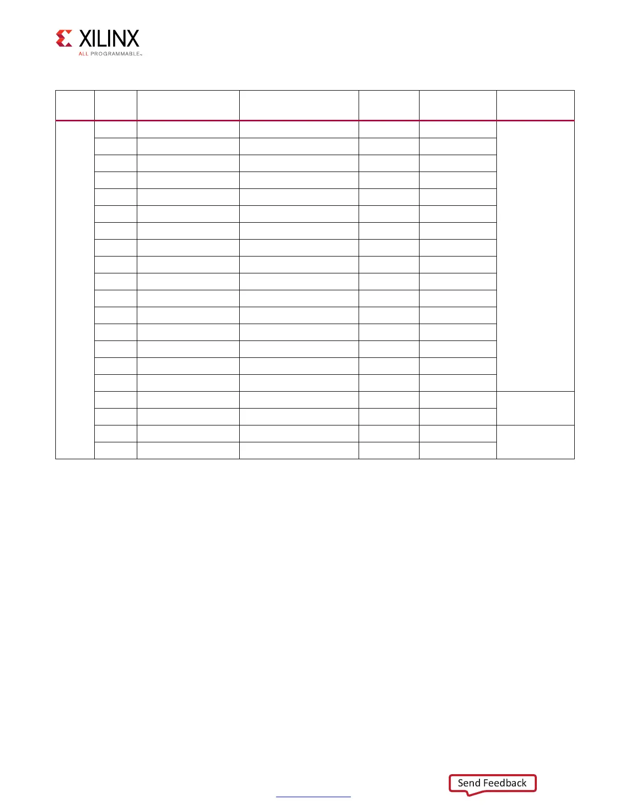
Table 3-20: VCU118 FPGA U1 GTY Transceiver Bank 233 Connections
MGT
Bank
FPGA
(U1) Pin
FPGA (U1) Pin Name Schematic Net Name
Connected
Pin
Connected Pin
Name
Connected
Device
GTY
Bank
233
G5 MGTYTXP0_233 FIREFLY_TX1_P A3 TX1P
QSFP2 U123
G4 MGTYTXN0_233 FIREFLY_TX1_N A2 TX1N
K2 MGTYRXP0_233 FIREFLY_RX1_P B17 RX1P
K1 MGTYRXN0_233 FIREFLY_RX1_N B18 RX1N
F7 MGTYTXP1_233 FIREFLY_TX2_P B3 TX2P
F6 MGTYTXN1_233 FIREFLY_TX2_N B2 TX2N
H2 MGTYRXP1_233 FIREFLY_RX2_P A17 RX2P
H1 MGTYRXN1_233 FIREFLY_RX2_N A18 RX2N
E5 MGTYTXP2_233 FIREFLY_TX3_P A6 TX3P
E4 MGTYTXN2_233 FIREFLY_TX3_N A5 TX3N
F2 MGTYRXP2_233 FIREFLY_RX3_P B14 RX3P
F1 MGTYRXN2_233 FIREFLY_RX3_N B15 RX3N
C5 MGTYTXP3_233 FIREFLY_TX4_P B6 TX4P
C4 MGTYTXN3_233 FIREFLY_TX4_N B5 TX4N
D2 MGTYRXP3_233 FIREFLY_RX4_P A14 RX4P
D1 MGTYRXN3_233 FIREFLY_RX4_N A15 RX4N
L9 MGTREFCLK0P_233 MGT_SI570_CLOCK3_C_P 15 Q3_P
U104 SI53340
clock buffer
L8 MGTREFCLK0N_233 MGT_SI570_CLOCK3_C_N 16 Q3_N
J9 MGTREFCLK1P_233 MGT232_CLK1_P
(1)
J33 1
SMA Connectors
J33(P), J32(N)
J8 MGTREFCLK1N_233 MGT232_CLK1_N
(1)
J32 1
Notes:
1. Ensure that the GTY RefClock being sourced into the RefClock SMAs (J32, J33) is AC coupled for proper clocking operation of
GTY transceivers. Use inline SMA DC blocking capacitors if frequency source output is not AC coupled.

 Loading...


