VCU118 Board User Guide 81
UG1224 (v1.0) December 15, 2016
www.xilinx.com
Chapter 3: Board Component Descriptions
Table 3-26 lists the FPGA U1 connections to dual-UART U34.
For more technical information on the CP2105GM and the VCP drivers, see the Silicon Labs
website [Ref 12].
Xilinx UART IP is expected to be implemented in the FPGA logic using IP. See the AXI UART
Lite LogiCORE IP Product Guide (PG142) [Ref 10] for more information.
I2C Bus, Topology, and Switches
[Figure 2-1, callouts 22, 23]
The VCU118 evaluation board implements a 2-to-1 I
2
C bus arrangement. The FPGA U1 HP
bank 64 (VCCO VCC1V8_FPGA) and system controller are wired to the same
IIC_MAIN_SDA/SCL I²C bus. The common I²C bus is then routed to a pair of 1-to-8 channel
TI TCA9548 bus switches U28 (address 0x74) and U80 (address 0x75). The bus switches can
operate at speeds up to 400 kHz. The VCU118 evaluation board I²C bus topology overview
is shown in Figure 3-18.
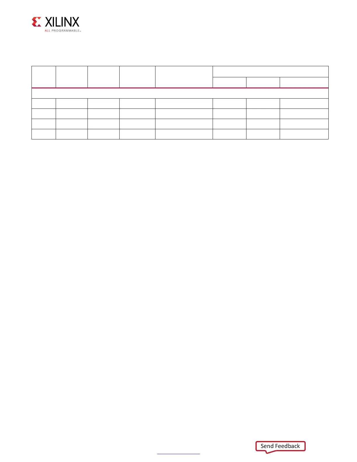
Table 3-26: FPGA U1 to CP2105GM U34 Connections
FPGA
(U1) Pin
Function Direction
I/O
Standard
Schematic Net
Name
CP2105GM Device (U34)
Pin Function Direction
The USB UART signal nets are named from the perspective of the CP2105GM device (U34)
AW25 RX Input LVCMOS18 USB_UART_TX 21 TXD Output
BB21 TX Output LVCMOS18 USB_UART_RX 20 RXD Input
AY25 CTS Input LVCMOS18 USB_UART_RTS 19 RTS Output
BB22 RTS Output LVCMOS18 USB_UART_CTS 18 CTS Input

 Loading...


