VCU118 Board User Guide 82
UG1224 (v1.0) December 15, 2016
www.xilinx.com
Chapter 3: Board Component Descriptions
IMPORTANT: The TCA9548 U28 and U80 RESET_B pin 3 is connected to FPGA U1 Bank 64 pin AL25.
FPGA pin AL25 LVCMOS18 net IIC_MUX_RESET_B must be driven High to enable I²C bus transactions
with the devices connected to U28 and U80.
User applications that communicate with devices on one of the downstream I
2
C buses must
first set up a path to the desired target bus through the U28 or U80 bus switch at I
2
C
address 0x74 (0b1110100) or 0x75 (0b111101), respectively. Table 3-27 lists the address
for each bus.
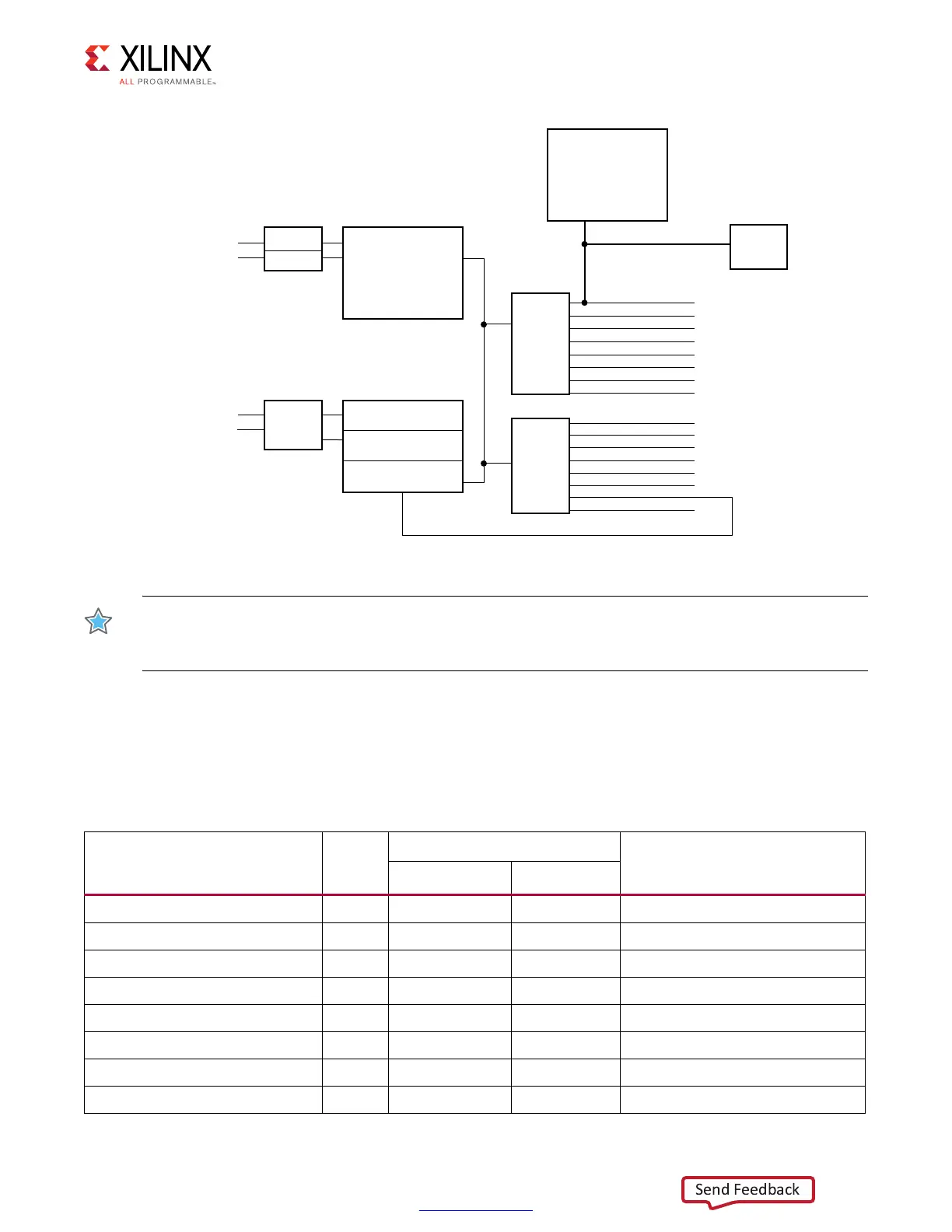
X-Ref Target - Figure 3-18
Figure 3-18: VCU118 IIC Bus
SYS Controller
U111
Level
shifters
always
enabled
SYS_1V8
BANK 501
Level
shifter
always
enabled
UTIL_3V3 to SYS_1V8
U109
MAXIM_CABLE_B
PMBUS_ALERT
MAXIM_CABLE_B
PMBUS_ALERT
UTIL_3V3 to VCC1V2_FPGA
Q27
IIC MUX1
TCA9548
PMBUS
FMCP_HSPC
FMC_HPC1
EEPROM
0x75
0x11-0x1B, 0x70-0x73
0xx##
0xx##
0x50
IIC MUX1
TCA9548
0x74
SI570 x1
NC
QSFPI
0x5D
0x50
SI570_0
SYSMON
0x68
0x5D
0x32
SI5328
Maxim power
regulators
12V_SW
Maxim
Cable
PMBUS SDA, SCL
0x10 – 0x18
U80
U28
Q23
Q21
UTIL_3V3 to
VCC1V8_FPGA
BANK 42
VCC1V2_FPGA
VCC1V8_FPGA
BANK 64
BANK 65
VCC1V8_FPGA
SYSMON IIC
FPGA U1
IIC_MAIN
INA_PMBUS
SI570_2
NC
0x40-0x45, 0x48
0x5D
NC
FIREFLY
QSFP2
0x50
0x50
X18025-102616
Table 3-27: I
2
C Bus Addresses
I
2
C Devices
I
2
C
Switch
Position
I
2
C Address
Device
Binary Format Hex Format
TCA9548 8-Channel bus switch N/A 0b1110100 0x74 U28 TCA9548
SI570_1 clock 0 0b1011101 0x5D U32 SI570
Not used 1 N/A N/A N/A
QSFP1 module 2 0b1010000 0x50 U145 28 Gb/s QSFP+
QSFP2 module 3 0b1010000 0x50 U123 28 Gb/s QSFP+
SI5328 clock 4 0b1101000 0x68 U57 SI5328B
SI570_0 clock 5 0b1011101 0x5D U18 SI570
FPGA SYSMON 6 0b0110010 0x32 U1 BANK 65

 Loading...


