VCU118 Board User Guide 40
UG1224 (v1.0) December 15, 2016
www.xilinx.com
Chapter 3: Board Component Descriptions
Digilent USB JTAG Module
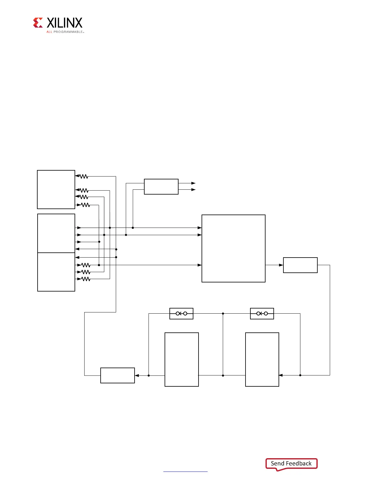
[Figure 2-1, callout 8, 9]
JTAG configuration is provided through a Digilent onboard USB-to-JTAG configuration
logic module (U115) where a host computer accesses the VCU118 board JTAG chain
through a type-A (host side) to micro-B (VCU118 board side J106) USB cable.
A 2 mm JTAG header (J3) is also provided in parallel for access by Xilinx download cables,
such as the Platform Cable USB II. JTAG initiated configuration takes priority over the
configuration method selected through the FPGA mode pins M[2:0], wired to SW16
positions [2:4]. The JTAG chain of the VCU118 board is illustrated in Figure 3-3.
For more details about the Digilent USB JTAG Module, see the Digilent website [Ref 21].
X-Ref Target - Figure 3-3
Figure 3-3: JTAG Chain Block Diagram
Digilent
USB
Module
(U115)
TCK
TMS
TDI
TDO
JTAG
Con
(J3)
TDO
TDI
TMS
TCK
1.8V 3.3V
U19
FPGA
TCK
TMS
TDI TDO
1.8V 3.3V
U19
Level-shifted to 3.3V
FMC
HPC1
Connector
TDITDO
FMC+
HSPC
Connector
TDITDO
1.8V 3.3V
U13
Level-shifted to 1.8V
J2 J22
SPST Bus Switch
U132
SPST Bus Switch
U26
N.C. N.C.
Level-shifted to 3.3V
To FMC HSPC J22
and FMC HPC1 J2
U1
System
Ctlr.
(U111)
TDO
TCK
TMS
TDI
X18023-100416

 Loading...


