VCU118 Board User Guide 51
UG1224 (v1.0) December 15, 2016
www.xilinx.com
Chapter 3: Board Component Descriptions
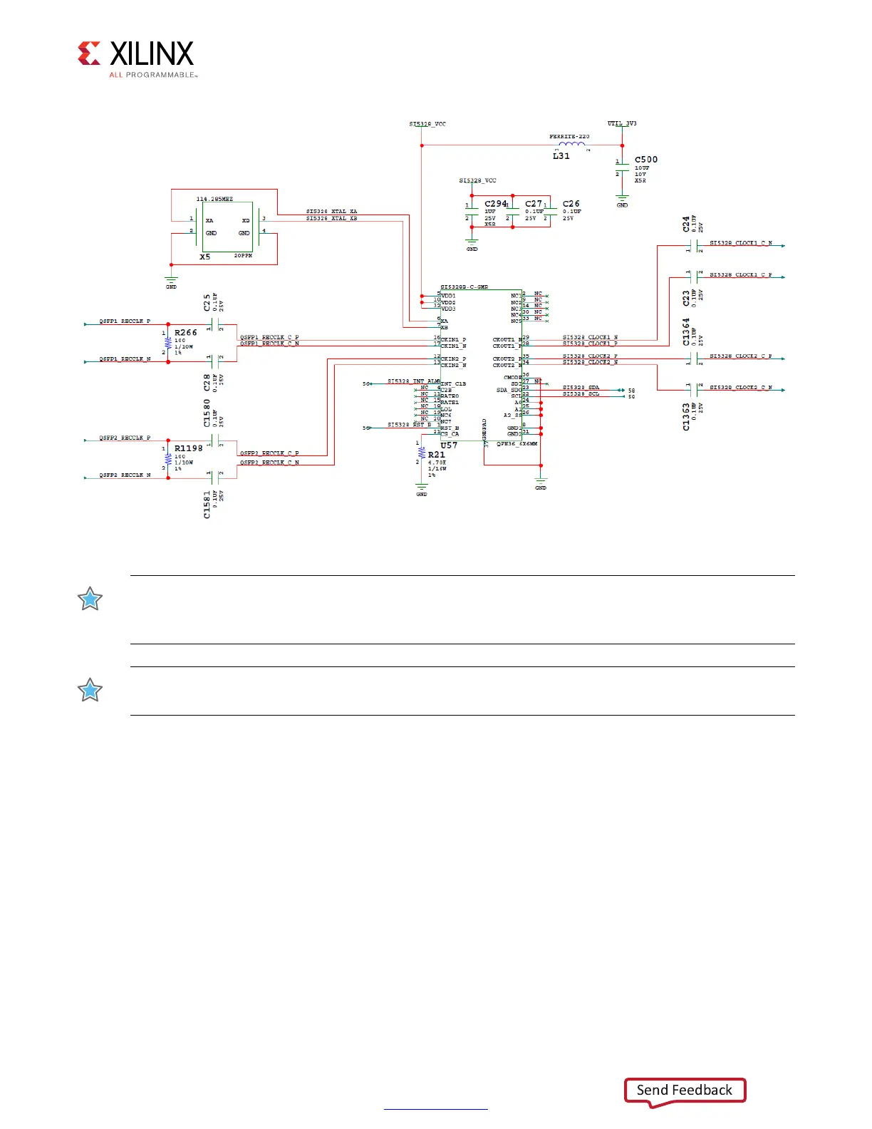
IMPORTANT: The Silicon Labs Si5328 U57 pin 1 reset net SI5328_RST_B must be driven High to enable
the device. U57 pin 1 net SI5328_RST_B is level-shifted to 1.8V by U3 and is connected to FPGA U1 bank
64 pin BC21.
IMPORTANT: The Silicon Labs Si5328 U57 component implements a 3-to-1 multiplexer. One of three
input clocks (XA/B, CKIN1, or CKIN2) is selected via I²C programming.
An active-Low input at U57 pin 1 RST_B performs an external hardware reset of this device.
This resets all internal logic to a known state and forces the device registers to their default
value. The clock outputs are disabled during reset. The part must be programmed after a
reset or a power-on to get a clock output. The reset pin 1 has a weak internal pull-up.
For more details on the Silicon Labs SI5335A, SI570, SI53340, and SI5328B devices, see the
Silicon Labs website [Ref 22].
For UltraScale FPGA clocking information, see UltraScale Architecture Clocking Resources
User Guide (UG572) [Ref 5].
X-Ref Target - Figure 3-9
Figure 3-9: VCU118 Board QSFP Jitter Attenuated Clock

 Loading...


