VCU118 Board User Guide 41
UG1224 (v1.0) December 15, 2016
www.xilinx.com
Chapter 3: Board Component Descriptions
FMC Connector JTAG Bypass
When an FMC is attached to the VCU118 board, it is automatically added to the JTAG chain
through electronically controlled single-pole single-throw (SPST) switches U26 (HSPC) and
U132 (HPC1). The SPST switches are in a normally closed state and transition to an open
state when the FMC is attached. Switch U26 adds an attached FMC to the FPGAs JTAG chain
as determined by the FMC_HSPC_H_PRSNT_M2C_B signal. Switch U132 adds an attached
FMC to the FPGAs JTAG chain as determined by the FMC_HPC1_PRSNT_M2C_B signal.
IMPORTANT: The attached FMC must implement a TDI-to-TDO connection through a device or bypass
jumper to ensure that the JTAG chain connects to the FPGA U1.
The JTAG connectivity on the VCU118 board allows a host computer to download bitstreams
to the FPGA using the Xilinx tools. In addition, the JTAG connector allows debug tools such
as the Vivado serial I/O analyzer or a software debugger to access the FPGA. The Xilinx tools
can also program the BPI parallel flash memory.
Clock Generation
[Figure 2-1, callout 10]
The VCU118 evaluation board provides multiple clock sources to the FPGA as listed in
Table 3-6.
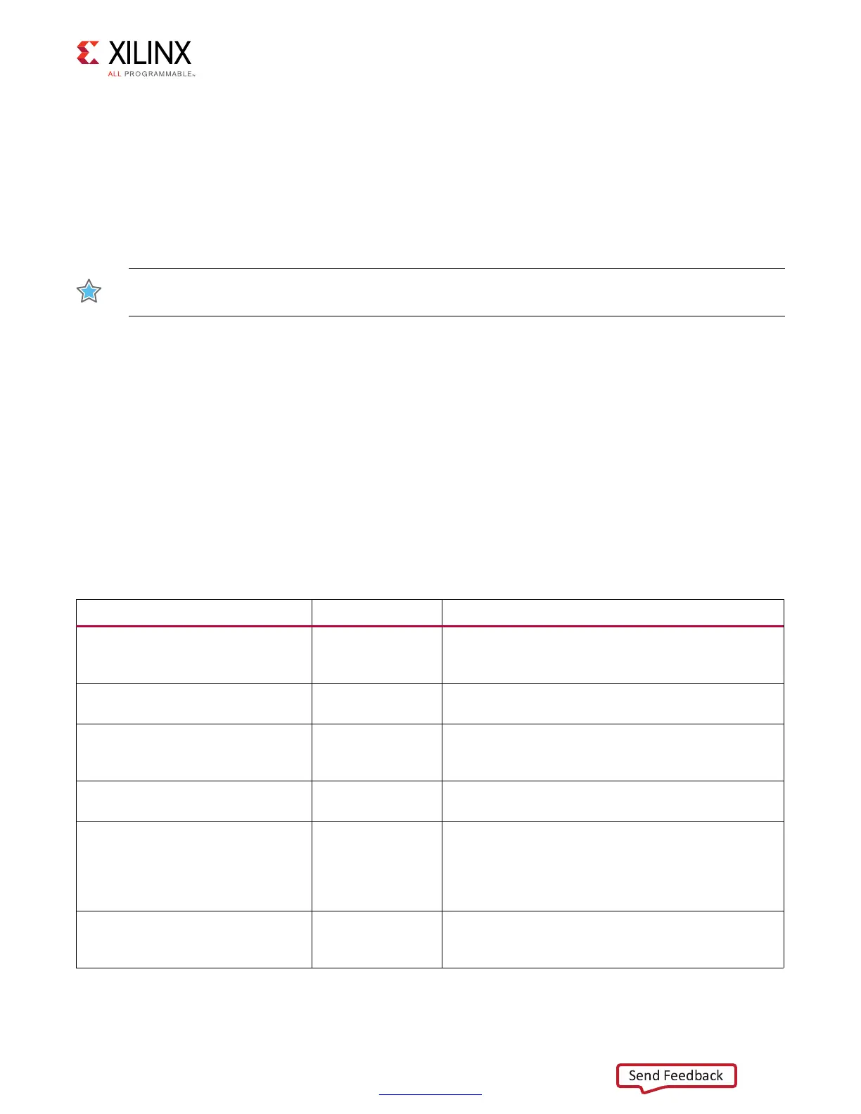
Table 3-6: VCU118 Board Clock Sources
Clock Name Clock Ref. Des. Description
System clock 300 MHz U122/U157
Silicon Labs Si5335A 1.8V LVDS any frequency quad
clock generator CLK0 drives U157 clock buffer.
(SYSCLK1_300_P/N)
System clock 125 MHz U122
Silicon Labs Si5335A 1.8V LVDS any frequency quad
clock generator CLK1. (CLK_125 MHz)
EMC clock 90 MHz U122
Silicon Labs Si5335A 1.8V LVCMOS single-ended any
frequency quad clock generator CLK2.
(FPGA_EMCCLK)
System control clock 33.333 MHz U122
Silicon Labs Si5335A 1.8V LVCMOS single-ended any
frequency quad clock generator CLK3. (SYSCTLR_CLK)
User clock 10 MHz-810 MHz U32/U104
Silicon Labs Si570 3.3V LVDS I
2
C programmable
oscillator, 156.250 MHz default. U32 output Q0 drives
U104 quad clock buffer. (US-ER_SI570_CLOCK_P/N
and MGT_SI570_CLOCK1_P/N through
MGT_SI570_CLOCK3_P/N)
QSFP1 Jitter attenuated clock U57
Silicon Labs Si5328B LVDS precision clock
multiplier/jitter attenuator. See Jitter Attenuated
Clock (SI5328_OUT1_P/N)

 Loading...


